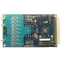
EVAL-AD7689EDZ Analog Devices Inc, EVAL-AD7689EDZ Datasheet - Page 29
EVAL-AD7689EDZ
Manufacturer Part Number
EVAL-AD7689EDZ
Description
BOARD EVAL AD7689
Manufacturer
Analog Devices Inc
Series
PulSAR®r
Specifications of EVAL-AD7689EDZ
Number Of Adc's
1
Number Of Bits
16
Sampling Rate (per Second)
250k
Data Interface
Serial
Inputs Per Adc
8 Single Ended
Input Range
±VREF
Power (typ) @ Conditions
12.5mW @ 250kSPS, 5 V
Voltage Supply Source
Single Supply
Operating Temperature
-40°C ~ 85°C
Utilized Ic / Part
AD7689
Silicon Manufacturer
Analog Devices
Application Sub Type
ADC
Kit Application Type
Data Converter
Silicon Core Number
AD7689
Lead Free Status / RoHS Status
Lead free / RoHS Compliant


READ/WRITE SPANNING CONVERSION WITH A
BUSY INDICATOR
This mode is used when the AD7682/AD7689 are connected to
any host using an SPI, serial port, or FPGA with an interrupt
input. The connection diagram is shown in Figure 42, and the
corresponding timing is given in Figure 43. For the SPI, the
host should use CPHA = CPOL = 1. Reading/writing spanning
conversion is shown, which covers all three modes detailed in
the Digital Interface section.
A rising edge on CNV initiates a conversion, ignores data
present on DIN and forces SDO to high impedance. After the
conversion is initiated, it continues until completion irrespec-
tive of the state of CNV. CNV must be returned low before the
safe data transfer time, t
conversion time, t
When the conversion is complete, SDO transitions from high
impedance to low (data ready), and with a pull-up to VIO, SDO
can be used to interrupt the host to begin data transfer.
After the conversion is complete, the AD7682/AD7689 enter
the acquisition phase and power-down. The host must enable
the MSB of the CFG register at this time (if necessary) to begin
CONVERSION
NOTES:
1. THE LSB IS FOR CONVERSION RESULTS OR THE CONFIGURATION REGISTER CFG (n – 1) IF
CNV
SDO
16 SCK FALLING EDGES = LSB OF CONVERSION RESULTS.
30 SCK FALLING EDGES = LSB OF CONFIGURATION REGISTER.
ON THE 17TH OR 31st SCK FALLING EDGE, SDO IS DRIVEN TO HIGH IMPENDANCE.
OTHERWISE, THE LSB REMAINS ACTIVE UNTIL THE BUSY INDICATOR IS DRIVEN LOW.
SCK
DIN
(n – 1)
CONV
t
SCKH
END DATA (n – 2)
, to generate the busy signal indicator.
t
SCKL
END CFG (n)
DATA
CONVERSION (n – 1)
t
15
DATA
X
t
SCK
, and then held low beyond the
16
LSB
X
+ 1
17/
31
X
LSB
Figure 43. Serial Interface Timing for the AD7682/AD7689 with a Busy Indicator
Figure 42. Connection Diagram for the AD7682/AD7689 with a Busy Indicator
t
DIS
(QUIET
TIME)
t
UPDATE (n)
EN
t
CFG/SDO
CYC
AD7682/
AD7689
BEIGN CFG (n + 1)
FOR SPI USE CPHA = 1, CPOL = 1.
CFG
MSB
MSB
CNV
SCK
1
SDO
DIN
t
SDIN
BEGIN DATA (n – 1)
Rev. B | Page 29 of 32
MSB –1
CFG
MSB
t
– 1
HDIN
ACQUISITION (n)
2
t
ACQ
VIO
t
t
HSDO
DSDO
the CFG update. While CNV is low, both a CFG update and a
data readback take place. The first 14 SCK rising edges are used to
update the CFG register, and the first 16 SCK falling edges clock
out the conversion results starting with the MSB. The restric-
tion for both configuring and reading is that they both occur
before the t
CFG[13:0] must be written or they are ignored. Also, if the 16-bit
conversion result is not read back before t
The SDO data is valid on both SCK edges. Although the rising
edge can be used to capture the data, a digital host using the
SCK falling edge allows a faster reading rate, provided it has an
acceptable hold time. After the optional 17
falling edge, SDO returns to high impedance. Note that if the
optional SCK falling edge is not used, the busy feature cannot
be detected, as described in the General Timing with a Busy
Indicator section.
If CFG readback is enabled, the CFG register associated with
the conversion result is read back MSB first following the LSB of
the conversion result. A total of 31 SCK falling edges is required
to return SDO to high impedance if this is enabled.
SCK
MISO
IRQ
SS
MOSI
DIGITAL HOST
DATA
t
t
CNVH
EN
time elapses for the next conversion. All 14 bits of
t
DIS
END DATA (n – 1)
END CFG (n + 1)
t
CONVERSION (n)
15
X
DATA
t
CONV
16
LSB
SEE NOTE
X
+ 1
SEE NOTE
17/
31
LSB
X
AD7682/AD7689
DATA
t
DIS
th
(or 31
(QUIET
TIME)
UPDATE (n + 1)
elapses, it is lost.
t
EN
CFG/SDO
st
ACQUISITION
) SCK
(n + 1)
Related parts for EVAL-AD7689EDZ
Image
Part Number
Description
Manufacturer
Datasheet
Request
R


Part Number:
Description:
BOARD EVAL FOR SI270X-A
Manufacturer:
Silicon Laboratories Inc
Datasheet:

Part Number:
Description:
BUCK CONV REF DESIGN KIT IP1201
Manufacturer:
International Rectifier
Datasheet:
Part Number:
Description:
BOARD DEMO SYNC DUAL BUCK CNVTER
Manufacturer:
International Rectifier
Datasheet:
Part Number:
Description:
BOARD DEMO SYNC BUCK CONVETER
Manufacturer:
International Rectifier
Datasheet:

Part Number:
Description:
EVALBOARD/EB Omnidirectional microphone - Analog
Manufacturer:
Analog Devices
Datasheet:
Part Number:
Description:
EVALBOARD/EB Omnidirectional microphone - Analog
Manufacturer:
Analog Devices
Datasheet:


Part Number:
Description:
BOARD EVAL LED DRIVER LT3756
Manufacturer:
Linear Technology
Datasheet:

Part Number:
Description:
BOARD EVAL FOR AD7741/7742
Manufacturer:
Analog Devices Inc
Datasheet:

Part Number:
Description:
±1.7g Dual-Axis IMEMS Accelerometer Evaluation Board
Manufacturer:
Analog Devices Inc
Datasheet:

Part Number:
Description:
IC MULTIPLIER ANALOG 8-SOIC T/R
Manufacturer:
Analog Devices Inc
Datasheet:

Part Number:
Description:
IC ANALOG MULTIPLIER 8-DIP
Manufacturer:
Analog Devices Inc
Datasheet:
Part Number:
Description:
IC ANALOG MULTIPLIER 8-SOIC
Manufacturer:
Analog Devices Inc
Datasheet:
Part Number:
Description:
IC ANALOG MULTIPLIER 8-DIP
Manufacturer:
Analog Devices Inc
Datasheet: