EVAL-AD7679CBZ Analog Devices Inc, EVAL-AD7679CBZ Datasheet - Page 10
EVAL-AD7679CBZ
Manufacturer Part Number
EVAL-AD7679CBZ
Description
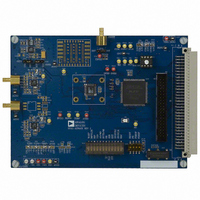
BOARD EVALUATION FOR AD7679
Manufacturer
Analog Devices Inc
Series
PulSAR®r
Specifications of EVAL-AD7679CBZ
Number Of Adc's
1
Number Of Bits
18
Sampling Rate (per Second)
570k
Data Interface
Serial, Parallel
Inputs Per Adc
1 Differential
Input Range
±VREF
Power (typ) @ Conditions
89mW @ 500kSPS
Voltage Supply Source
Analog and Digital
Operating Temperature
-40°C ~ 85°C
Utilized Ic / Part
AD7679
Lead Free Status / RoHS Status
Lead free / RoHS Compliant


AD7679
Pin No.
34
35
36
37
38
39
43
46
48
49
(EPAD)
1
Table 7. Data Bus Interface Definitions
MODE
0
1
1
2
2
2
2
3
R[0:17] is the 18-bit ADC value stored in its output register.
AI = Analog Input; AO = Analog Output; DI = Digital Input; DI/O = Bidirectional Digital; DO = Digital Output; P = Power.
MODE1
0
0
0
1
1
1
1
1
Mnemonic
PD
CNVST
AGND
REF
REFGND
IN–
IN+
REFBUFIN
PDBUF
Exposed Pad
(EPAD)
MODE0
0
1
1
0
0
0
0
1
Type
DI
DI
P
AI
AI
AI
AI
AI
DI
D0/OB/2C
R[0]
OB/2C
OB/2C
OB/2C
OB/2C
OB/2C
OB/2C
OB/2C
1
Description
Power-Down Input. When set to a logic HIGH, power consumption is reduced and conversions are
inhibited after the current one is completed.
Start Conversion. If CNVST is held HIGH when the acquisition phase (t
edge on CNVST puts the internal sample/hold into the hold state and initiates a conversion. If CNVST
is held LOW when the acquisition phase is complete, the internal sample/hold is put into the hold
state and a conversion is started immediately.
Must Be Tied to Analog Ground.
Reference Input Voltage and Internal Reference Buffer Output. Apply an external reference on this pin
if the internal reference buffer is not used. Should be decoupled effectively with or without the
internal buffer.
Reference Input Analog Ground.
Differential Negative Analog Input.
Differential Positive Analog Input.
Reference Buffer Input Voltage. The internal reference buffer has a fixed gain. It outputs 4.096 V
typically when 2.5 V is applied on this pin.
Allows Choice of Buffering Reference. When LOW, buffer is selected. When HIGH, buffer is
switched off.
The exposed pad is internally connected to AGND. This connection is not required to meet the
electrical performances however, for increased reliability of the solder joints, it is recommended
that the pad be soldered to the analog ground of the
D1/A0
R[1]
A0:0
A0:1
A0:0
A0:0
A0:1
A0:1
All Hi-Z
D2/A1
R[2]
R[2]
R[0]
A1:0
A1:1
A1:0
A1:1
Rev. A | Page 10 of 28
D[3]
R[3]
R[3]
R[1]
All Hi-Z
All Hi-Z
All Hi-Z
All Hi-Z
D[4:9]
R[4:9]
R[4:9]
D[10:11]
R[10:11]
R[10:11]
R[10:11]
R[2:3]
R[0:1]
Serial Interface
All Zeros
All Zeros
system.
D[12:15]
R[12:15]
R[12:15]
R[12:15]
R[4:7]
All Zeros
D[16:17]
R[16:17]
R[16:17]
R[16:17]
R[8:9]
R[0:1]
8
) is complete, the next falling
Description
18-Bit Parallel
16-Bit High Word
16-Bit Low Word
8-Bit HIGH Byte
8-Bit MID Byte
8-Bit LOW Byte
8-Bit LOW Byte
Serial Interface
Related parts for EVAL-AD7679CBZ
Image
Part Number
Description
Manufacturer
Datasheet
Request
R


Part Number:
Description:
BOARD EVAL FOR SI270X-A
Manufacturer:
Silicon Laboratories Inc
Datasheet:

Part Number:
Description:
BUCK CONV REF DESIGN KIT IP1201
Manufacturer:
International Rectifier
Datasheet:
Part Number:
Description:
BOARD DEMO SYNC DUAL BUCK CNVTER
Manufacturer:
International Rectifier
Datasheet:
Part Number:
Description:
BOARD DEMO SYNC BUCK CONVETER
Manufacturer:
International Rectifier
Datasheet:

Part Number:
Description:
EVALBOARD/EB Omnidirectional microphone - Analog
Manufacturer:
Analog Devices
Datasheet:
Part Number:
Description:
EVALBOARD/EB Omnidirectional microphone - Analog
Manufacturer:
Analog Devices
Datasheet:


Part Number:
Description:
BOARD EVAL LED DRIVER LT3756
Manufacturer:
Linear Technology
Datasheet:

Part Number:
Description:
BOARD EVAL FOR AD7741/7742
Manufacturer:
Analog Devices Inc
Datasheet:

Part Number:
Description:
±1.7g Dual-Axis IMEMS Accelerometer Evaluation Board
Manufacturer:
Analog Devices Inc
Datasheet:

Part Number:
Description:
IC MULTIPLIER ANALOG 8-SOIC T/R
Manufacturer:
Analog Devices Inc
Datasheet:

Part Number:
Description:
IC ANALOG MULTIPLIER 8-DIP
Manufacturer:
Analog Devices Inc
Datasheet:
Part Number:
Description:
IC ANALOG MULTIPLIER 8-SOIC
Manufacturer:
Analog Devices Inc
Datasheet:
Part Number:
Description:
IC ANALOG MULTIPLIER 8-DIP
Manufacturer:
Analog Devices Inc
Datasheet: