EVAL-AD7679CBZ Analog Devices Inc, EVAL-AD7679CBZ Datasheet - Page 9
EVAL-AD7679CBZ
Manufacturer Part Number
EVAL-AD7679CBZ
Description
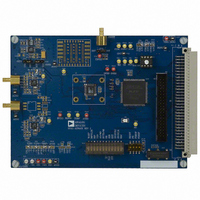
BOARD EVALUATION FOR AD7679
Manufacturer
Analog Devices Inc
Series
PulSAR®r
Specifications of EVAL-AD7679CBZ
Number Of Adc's
1
Number Of Bits
18
Sampling Rate (per Second)
570k
Data Interface
Serial, Parallel
Inputs Per Adc
1 Differential
Input Range
±VREF
Power (typ) @ Conditions
89mW @ 500kSPS
Voltage Supply Source
Analog and Digital
Operating Temperature
-40°C ~ 85°C
Utilized Ic / Part
AD7679
Lead Free Status / RoHS Status
Lead free / RoHS Compliant


Pin No.
13
14
15
16
17
18
19
20
21
22
23
24
25–28
29
30
31
32
33
Mnemonic
D6
or EXT/INT
D7
or INVSYNC
D8
or INVSCLK
D9
or RDC/SDIN
OGND
OVDD
DVDD
DGND
D10
or SDOUT
D11
or SCLK
D12
or SYNC
D13
or RDERROR
D[14:17]
BUSY
DGND
RD
CS
RESET
Type
DI/O
DI/O
DI/O
DI/O
P
P
P
P
DO
DI/O
DO
DO
DO
DO
P
DI
DI
DI
1
Description
In all modes except MODE = 3, this output is used as Bit 6 of the parallel port data output bus.
When MODE = 3 (serial mode), this input, part of the serial port, is used as a digital select input for
choosing the internal data clock or an external data clock. With EXT/INT tied LOW, the internal clock is
selected on the SCLK output. With EXT/INT set to a logic HIGH, output data is synchronized to an
external clock signal connected to the SCLK input.
In all modes except MODE = 3, this output is used as Bit 7 of the parallel port data output bus.
When MODE = 3 (serial mode), this input, part of the serial port, is used to select the active state of the
SYNC signal. When LOW, SYNC is active HIGH. When HIGH, SYNC is active LOW.
In all modes except MODE = 3, this output is used as Bit 8 of the parallel port data output bus.
When MODE = 3 (serial mode), this input, part of the serial port, is used to invert the SCLK signal. It is
active in both master and slave mode.
In all modes except MODE = 3, this output is used as Bit 9 of the parallel port data output bus.
When MODE = 3 (serial mode), this input, part of the serial port, is used as either an external data
input or a read mode selection input depending on the state of EXT/INT. When EXT/ INT is HIGH,
RDC/SDIN could be used as a data input to daisy-chain the conversion results from two or more ADCs
onto a single SDOUT line. The digital data level on SDIN is output on SDOUT with a delay of 18 SCLK
periods after the initiation of the read sequence. When EXT/INT is LOW, RDC/SDIN is used to select the
read mode. When RDC/SDIN is HIGH, the data is output on SDOUT during conversion. When RDC/SDIN
is LOW, the data can be output on SDOUT only when the conversion is complete.
Input/Output Interface Digital Power Ground.
Output Interface Digital Power. Nominally at the same supply as the host interface (5 V or 3 V). Should
not exceed DVDD by more than 0.3 V.
Digital Power. Nominally at 5 V.
Digital Power Ground.
In all modes except MODE = 3, this output is used as Bit 10 of the parallel port data output bus.
When MODE = 3 (serial mode), this output, part of the serial port, is used as a serial data output
synchronized to SCLK. Conversion results are stored in an on-chip register. The AD7679 provides the
conversion result, MSB first, from its internal shift register. The data format is determined by the logic
level of OB/2C. In serial mode when EXT/INT is LOW, SDOUT is valid on both edges of SCLK. In serial
mode when EXT/INT is HIGH and INVSCLK is LOW, SDOUT is updated on the SCLK rising edge and is
valid on the next falling edge; if INVSCLK is HIGH, SDOUT is updated on the SCLK falling edge and is
valid on the next rising edge.
In all modes except MODE = 3, this output is used as Bit 11 of the parallel port data output bus.
When MODE = 3 (serial mode), this pin, part of the serial port, is used as a serial data clock input or
output, dependent upon the logic state of the EXT/INT pin. The active edge where the data SDOUT is
updated depends upon the logic state of the INVSCLK pin.
In all modes except MODE = 3, this output is used as Bit 12 of the parallel port data output bus.
When MODE = 3 (serial mode), this output, part of the serial port, is used as a digital output frame
synchronization for use with the internal data clock (EXT/INT = Logic LOW). When a read sequence is
initiated and INVSYNC is LOW, SYNC is driven HIGH and remains HIGH while the SDOUT output is valid.
When a read sequence is initiated and INVSYNC is HIGH, SYNC is driven LOW and remains LOW while
SDOUT output is valid.
In all modes except MODE = 3, this output is used as Bit 13 of the parallel port data output bus.
In MODE = 3 (serial mode) and when EXT/ INT is HIGH, this output, part of the serial port, is used as an
incomplete read error flag. In slave mode, when a data read is started and not complete when the
following conversion is complete, the current data is lost and RDERROR is pulsed high.
Bit 14 to Bit 17 of the Parallel Port Data Output Bus. These pins are always outputs regardless of the
interface mode.
Busy Output. Transitions HIGH when a conversion is started. Remains HIGH until the conversion is
complete and the data is latched into the on-chip shift register. The falling edge of BUSY could be
used as a data ready clock signal.
Must Be Tied to Digital Ground.
Read Data. When CS and RD are both LOW, the interface parallel or serial output bus is enabled.
Chip Select. When CS and RD are both LOW, the interface parallel or serial output bus is enabled. CS is
also used to gate the external clock.
Reset Input. When set to a logic HIGH, reset the AD7679. Current conversion, if any, is aborted. If not
used, this pin could be tied to DGND.
Rev. A | Page 9 of 28
AD7679
Related parts for EVAL-AD7679CBZ
Image
Part Number
Description
Manufacturer
Datasheet
Request
R


Part Number:
Description:
BOARD EVAL FOR SI270X-A
Manufacturer:
Silicon Laboratories Inc
Datasheet:

Part Number:
Description:
BUCK CONV REF DESIGN KIT IP1201
Manufacturer:
International Rectifier
Datasheet:
Part Number:
Description:
BOARD DEMO SYNC DUAL BUCK CNVTER
Manufacturer:
International Rectifier
Datasheet:
Part Number:
Description:
BOARD DEMO SYNC BUCK CONVETER
Manufacturer:
International Rectifier
Datasheet:

Part Number:
Description:
EVALBOARD/EB Omnidirectional microphone - Analog
Manufacturer:
Analog Devices
Datasheet:
Part Number:
Description:
EVALBOARD/EB Omnidirectional microphone - Analog
Manufacturer:
Analog Devices
Datasheet:


Part Number:
Description:
BOARD EVAL LED DRIVER LT3756
Manufacturer:
Linear Technology
Datasheet:

Part Number:
Description:
BOARD EVAL FOR AD7741/7742
Manufacturer:
Analog Devices Inc
Datasheet:

Part Number:
Description:
±1.7g Dual-Axis IMEMS Accelerometer Evaluation Board
Manufacturer:
Analog Devices Inc
Datasheet:

Part Number:
Description:
IC MULTIPLIER ANALOG 8-SOIC T/R
Manufacturer:
Analog Devices Inc
Datasheet:

Part Number:
Description:
IC ANALOG MULTIPLIER 8-DIP
Manufacturer:
Analog Devices Inc
Datasheet:
Part Number:
Description:
IC ANALOG MULTIPLIER 8-SOIC
Manufacturer:
Analog Devices Inc
Datasheet:
Part Number:
Description:
IC ANALOG MULTIPLIER 8-DIP
Manufacturer:
Analog Devices Inc
Datasheet: