EVAL-AD7679CBZ Analog Devices Inc, EVAL-AD7679CBZ Datasheet - Page 18
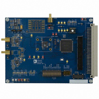
EVAL-AD7679CBZ
Manufacturer Part Number
EVAL-AD7679CBZ
Description
BOARD EVALUATION FOR AD7679
Manufacturer
Analog Devices Inc
Series
PulSAR®r
Specifications of EVAL-AD7679CBZ
Number Of Adc's
1
Number Of Bits
18
Sampling Rate (per Second)
570k
Data Interface
Serial, Parallel
Inputs Per Adc
1 Differential
Input Range
±VREF
Power (typ) @ Conditions
89mW @ 500kSPS
Voltage Supply Source
Analog and Digital
Operating Temperature
-40°C ~ 85°C
Utilized Ic / Part
AD7679
Lead Free Status / RoHS Status
Lead free / RoHS Compliant


AD7679
•
The AD8021 meets these requirements and is usually
appropriate for almost all applications. The AD8021 needs a
10 pF external compensation capacitor, which should have good
linearity as an NPO ceramic or mica type.
The AD8022 could be used if a dual version is needed and gain
of 1 is present. The AD829 is an alternative in applications
where high frequency (above 100 kHz) performance is not
required. In gain of 1 applications, it requires an 82 pF
compensation capacitor. The AD8610 is another option when
low bias current is needed in low frequency applications.
Single-to-Differential Driver
For applications using unipolar analog signals, a single-ended-
to-differential driver will allow for a differential input into the
part. The schematic is shown in Figure 29. When provided an
input signal of 0 to V
differential ±V
The SNR degradation due to the amplifier is
where:
f
(26 MHz) or the cutoff frequency of the input filter, if used.
N is the noise factor of the amplifiers (1 if in buffer
configuration).
e
nV/√Hz.
For instance, for a driver with an equivalent input noise of
2 nV/√Hz (e.g., AD8021) configured as a buffer, thus with
a noise gain of +1, the SNR degrades by only 0.34 dB with
the filter in Figure 25, and by 1.8 dB without it.
The driver needs to have a THD performance suitable to
that of the AD7679.
–3dB
N
is the equivalent input noise voltage of each op amp in
is the –3 dB input bandwidth in MHz of the AD7679
SNR
REF
LOSS
with midscale at V
REF
=
20
, this configuration will produce a
log
⎛
⎜
⎜
⎜
⎜
⎜
⎝
625
+
REF
π
/2.
f
25
–
3dB
(
Ne
N
2 )
⎞
⎟
⎟
⎟
⎟
⎟
⎠
Rev. A | Page 18 of 28
If the application can tolerate more noise, the AD8138,
differential driver can be used.
Voltage Reference
The AD7679 allows the use of an external voltage reference
either with or without the internal reference buffer.
Using the internal reference buffer is recommended when
sharing a common reference voltage between multiple ADCs is
desired.
However, the advantages of using the external reference voltage
directly are
•
•
To use the internal reference buffer, PDBUF should be LOW. A
2.5 V reference voltage applied on the REFBUFIN input will
result in a 4.096 V reference on the REF pin.
In both cases, the voltage reference input REF has a dynamic
input impedance and therefore requires an efficient decoupling
between REF and REFGND inputs. The decoupling consists of
a low ESR 47 μF tantalum capacitor connected to the REF and
REFGND inputs with minimum parasitic inductance.
Care should also be taken with the reference temperature
coefficient of the voltage reference, which directly affects the
full-scale accuracy if this parameter matters. For instance, a
±4 ppm/°C temperature coefficient of the reference changes the
full scale by ±1 LSB/°C.
ANALOG INPUT
0V TO 4.096V)
(UNIPOLAR
The SNR and dynamic range improvement (about 1.7 dB)
resulting from the use of a reference voltage very close to
the supply (5 V) instead of a typical 4.096 V reference
when the internal buffer is used.
The power saving when the internal reference buffer is
powered down (PDBUF high).
Figure 29. Single-Ended-to-Differential Driver Circuit
8.25kΩ
1.82k Ω
U1
(Internal Reference Buffer Used)
100nF
AD8021
10pF
590Ω
590Ω
U2
AD8021
10pF
2.7nF
30 Ω
30 Ω
2.7nF
IN+
IN– REF
AD7679
10 μ F
REFBUFIN
03085-0-031
2.5V
Related parts for EVAL-AD7679CBZ
Image
Part Number
Description
Manufacturer
Datasheet
Request
R


Part Number:
Description:
BOARD EVAL FOR SI270X-A
Manufacturer:
Silicon Laboratories Inc
Datasheet:

Part Number:
Description:
BUCK CONV REF DESIGN KIT IP1201
Manufacturer:
International Rectifier
Datasheet:
Part Number:
Description:
BOARD DEMO SYNC DUAL BUCK CNVTER
Manufacturer:
International Rectifier
Datasheet:
Part Number:
Description:
BOARD DEMO SYNC BUCK CONVETER
Manufacturer:
International Rectifier
Datasheet:

Part Number:
Description:
EVALBOARD/EB Omnidirectional microphone - Analog
Manufacturer:
Analog Devices
Datasheet:
Part Number:
Description:
EVALBOARD/EB Omnidirectional microphone - Analog
Manufacturer:
Analog Devices
Datasheet:


Part Number:
Description:
BOARD EVAL LED DRIVER LT3756
Manufacturer:
Linear Technology
Datasheet:

Part Number:
Description:
BOARD EVAL FOR AD7741/7742
Manufacturer:
Analog Devices Inc
Datasheet:

Part Number:
Description:
±1.7g Dual-Axis IMEMS Accelerometer Evaluation Board
Manufacturer:
Analog Devices Inc
Datasheet:

Part Number:
Description:
IC MULTIPLIER ANALOG 8-SOIC T/R
Manufacturer:
Analog Devices Inc
Datasheet:

Part Number:
Description:
IC ANALOG MULTIPLIER 8-DIP
Manufacturer:
Analog Devices Inc
Datasheet:
Part Number:
Description:
IC ANALOG MULTIPLIER 8-SOIC
Manufacturer:
Analog Devices Inc
Datasheet:
Part Number:
Description:
IC ANALOG MULTIPLIER 8-DIP
Manufacturer:
Analog Devices Inc
Datasheet: