EVAL-AD7679CBZ Analog Devices Inc, EVAL-AD7679CBZ Datasheet - Page 25
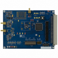
EVAL-AD7679CBZ
Manufacturer Part Number
EVAL-AD7679CBZ
Description
BOARD EVALUATION FOR AD7679
Manufacturer
Analog Devices Inc
Series
PulSAR®r
Specifications of EVAL-AD7679CBZ
Number Of Adc's
1
Number Of Bits
18
Sampling Rate (per Second)
570k
Data Interface
Serial, Parallel
Inputs Per Adc
1 Differential
Input Range
±VREF
Power (typ) @ Conditions
89mW @ 500kSPS
Voltage Supply Source
Analog and Digital
Operating Temperature
-40°C ~ 85°C
Utilized Ic / Part
AD7679
Lead Free Status / RoHS Status
Lead free / RoHS Compliant


APPLICATION HINTS
LAYOUT
The AD7679 has very good immunity to noise on the power
supplies. However, care should still be taken with regard to
grounding layout.
The printed circuit board that houses the AD7679 should be
designed so that the analog and digital sections are separated
and confined to certain areas of the board. This facilitates the
use of ground planes that can be easily separated. Digital and
analog ground planes should be joined in only one place,
preferably underneath the AD7679, or at least as close to the
AD7679 as possible. If the AD7679 is in a system where
multiple devices require analog-to-digital ground connections,
the connection should still be made at one point only, a star
ground point that should be established as close to the AD7679
as possible.
The user should avoid running digital lines under the device, as
these will couple noise onto the die. The analog ground plane
should be allowed to run under the AD7679 to avoid noise
coupling. Fast switching signals like CNVST or clocks should be
shielded with digital ground to avoid radiating noise to other
sections of the board, and should never run near analog signal
paths. Crossover of digital and analog signals should be
avoided. Traces on different but close layers of the board should
run at right angles to each other. This will reduce the effect of
feedthrough through the board. The power supply lines to the
AD7679 should use as large a trace as possible to provide low
impedance paths and reduce the effect of glitches on the power
supply lines. Good decoupling is also important to lower the
supply’s impedance presented to the AD7679 and to reduce the
magnitude of the supply spikes. Decoupling ceramic capacitors,
typically 100 nF, should be placed close to and ideally right up
against each power supply pin (AVDD, DVDD, and OVDD)
and their corresponding ground pins. Additionally, low ESR
10 μF capacitors should be located near the ADC to further
reduce low frequency ripple.
Rev. A | Page 25 of 28
The DVDD supply of the AD7679 can be a separate supply or
can come from the analog supply, AVDD, or the digital
interface supply, OVDD. When the system digital supply is
noisy or when fast switching digital signals are present, and if
no separate supply is available, the user should connect the
DVDD digital supply to the analog supply AVDD through an
RC filter, (see Figure 25), and connect the system supply to the
interface digital supply OVDD and the remaining digital
circuitry. When DVDD is powered from the system supply, it is
useful to insert a bead to further reduce high frequency spikes.
The AD7679 has four different ground pins: REFGND, AGND,
DGND, and OGND. REFGND senses the reference voltage and
should be a low impedance return to the reference because it
carries pulsed currents. AGND is the ground to which most
internal ADC analog signals are referenced. This ground must
be connected with the least resistance to the analog ground
plane. DGND must be tied to the analog or digital ground plane
depending on the configuration. OGND is connected to the
digital system ground.
The layout of the decoupling of the reference voltage is
important. The decoupling capacitor should be close to the
ADC and should be connected with short and large traces to
minimize parasitic inductances.
EVALUATING THE AD7679’S PERFORMANCE
An evaluation board for the AD7679 allows a quick means
to measure both dc (histograms and time domain) and ac (time
and frequency domain) performances of the converter. The
EVAL-AD7679CBZ is an evaluation board package that
includes a fully assembled and tested evaluation board,
documentation, and software. The accompanying software
requires the use of a capture board, which must be ordered
separately from the evaluation board (see the Ordering Guide
for information). The evaluation board can also be used in a
standalone configuration and does not use the software when
in this mode. Refer to the
AD76XXCBZ
evaluation board details.
Two types of data capture boards can be used with the EVAL-
AD7679CBZ:
•
•
The recommended board layout for the AD7679 is outlined in
the evaluation board data sheet.
USB based (EVAL-CED1Z recommended)
Parallel port based (EVAL-CONTROL BRD3Z not
recommended because many newer PCs do not include
parallel ports any longer)
data sheets available from
EVAL-AD76XXEDZ
www.analog.com
and
EVAL-
AD7679
for
Related parts for EVAL-AD7679CBZ
Image
Part Number
Description
Manufacturer
Datasheet
Request
R


Part Number:
Description:
BOARD EVAL FOR SI270X-A
Manufacturer:
Silicon Laboratories Inc
Datasheet:

Part Number:
Description:
BUCK CONV REF DESIGN KIT IP1201
Manufacturer:
International Rectifier
Datasheet:
Part Number:
Description:
BOARD DEMO SYNC DUAL BUCK CNVTER
Manufacturer:
International Rectifier
Datasheet:
Part Number:
Description:
BOARD DEMO SYNC BUCK CONVETER
Manufacturer:
International Rectifier
Datasheet:

Part Number:
Description:
EVALBOARD/EB Omnidirectional microphone - Analog
Manufacturer:
Analog Devices
Datasheet:
Part Number:
Description:
EVALBOARD/EB Omnidirectional microphone - Analog
Manufacturer:
Analog Devices
Datasheet:


Part Number:
Description:
BOARD EVAL LED DRIVER LT3756
Manufacturer:
Linear Technology
Datasheet:

Part Number:
Description:
BOARD EVAL FOR AD7741/7742
Manufacturer:
Analog Devices Inc
Datasheet:

Part Number:
Description:
±1.7g Dual-Axis IMEMS Accelerometer Evaluation Board
Manufacturer:
Analog Devices Inc
Datasheet:

Part Number:
Description:
IC MULTIPLIER ANALOG 8-SOIC T/R
Manufacturer:
Analog Devices Inc
Datasheet:

Part Number:
Description:
IC ANALOG MULTIPLIER 8-DIP
Manufacturer:
Analog Devices Inc
Datasheet:
Part Number:
Description:
IC ANALOG MULTIPLIER 8-SOIC
Manufacturer:
Analog Devices Inc
Datasheet:
Part Number:
Description:
IC ANALOG MULTIPLIER 8-DIP
Manufacturer:
Analog Devices Inc
Datasheet: