CDB5534U Cirrus Logic Inc, CDB5534U Datasheet - Page 15
CDB5534U
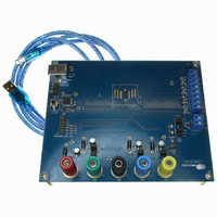
Manufacturer Part Number
CDB5534U
Description
EVAL BOARD FOR CS5534
Manufacturer
Cirrus Logic Inc
Specifications of CDB5534U
Number Of Adc's
1
Number Of Bits
24
Sampling Rate (per Second)
3.84k
Data Interface
Serial
Inputs Per Adc
2 Single
Input Range
0 ~ 2.5 V
Power (typ) @ Conditions
35mW @ 5 V
Voltage Supply Source
Analog and Digital, Dual ±
Operating Temperature
-40°C ~ 85°C
Utilized Ic / Part
CS5534
Description/function
Audio DSPs
Operating Supply Voltage
5 V
Product
Audio Modules
For Use With/related Products
C8051F320
Lead Free Status / RoHS Status
Contains lead / RoHS non-compliant
Lead Free Status / RoHS Status
Lead free / RoHS Compliant, Contains lead / RoHS non-compliant
Other names
598-1016


instruct the converter to perform single or multiple
conversions or calibrations with the converter in
the mode defined by one of these Setups.
Using the single conversion mode, an 8-bit com-
mand word can be written into the serial port. The
command includes pointer bits which ‘point’ to a
16-bit command in one of the Channel Setup Reg-
isters which is to be executed. The 16-bit Setups
can be programmed to perform a conversion on any
of the input channels of the converter. More than
one of the 16-bit Setups can be used for the same
analog input channel. This allows the user to con-
vert on the same signal with either a different con-
version speed, a different gain range, or any of the
other options available in the channel setup regis-
ters. Alternately, the user can set up the registers to
perform different conversion conditions on each of
the input channels.
The ADCs also include continuous conversion ca-
pability. The ADCs can be instructed to continu-
ously convert, referencing one 16-bit command
Setup. In the continuous conversions mode, the
conversion data words are loaded into a shift regis-
ter. The converter issues a flag on the SDO pin
when a conversion cycle is completed so the user
can read the register, if need be. See the section on
Performing Conversions for more details.
The following pages document how to initialize the
converter, perform offset and gain calibrations, and
how to configure the converter for the various con-
version modes. Each of the bits of the configuration
register and of the Channel Setup Registers is de-
scribed. A list of examples follows the description
section. Also the Command Register Quick Refer-
ence can be used to decode all valid commands (the
first 8-bits into the serial port).
2.2.1. System Initialization
The CS5531/32/33/34 provide no power-on-reset
function. To initialize the ADCs, the user must per-
form a software reset by resetting the ADC’s serial
port with the Serial Port Initialization sequence.
DS289F5
This sequence resets the serial port to the command
mode and is accomplished by transmitting at least
15 SYNC1 command bytes (0xFF hexadecimal),
followed by one SYNC0 command (0xFE hexa-
decimal). Note that this sequence can be initiated at
anytime to reinitialize the serial port. To complete
the system initialization sequence, the user must
also perform a system reset sequence which is as
follows: Write a logic 1 into the RS bit of the con-
figuration register. This will reset the calibration
registers and other logic (but not the serial port). A
valid reset will set the RV bit in the configuration
register to a logic 1. After writing the RS bit to a
logic 1, wait 20 microseconds, then write the RS bit
back to logic 0. While this involves writing an en-
tire word into the configuration register, the RV bit
is a read only bit, therefore a write to the configu-
ration register will not overwrite the RV bit. After
clearing the RS bit back to logic 0, read the config-
uration register to check the state of the RV bit as
this indicates that a valid reset occurred. Reading
the configuration register clears the RV bit back to
logic 0.
Completing the reset cycle initializes the on-chip
registers to the following states:
Note:
Configuration Register:
Offset Registers:
Gain Registers:
Channel Setup Registers: 00000000(H)
Previous datasheets stated that the RS bit
would clear itself back to logic 0 and therefore
the user was not required to write the RS bit
back to logic 0. The current data sheet
instruction that requires the user to write into
the configuration register to clear the RS bit
has been added to insure that the RS bit is
cleared. Characterization across multiple lots
of silicon has indicated some chips do not
automatically reset the RS bit to logic 0 in the
configuration register, although the reset
function is completed. This occurs only on
small number of chips when the VA- supply is
negative with respect to DGND. This has not
CS5531/32/33/34-AS
00000000(H)
00000000(H)
01000000(H)
15
Related parts for CDB5534U
Image
Part Number
Description
Manufacturer
Datasheet
Request
R

Part Number:
Description:
Development Kit
Manufacturer:
Cirrus Logic Inc
Datasheet:
Part Number:
Description:
Development Kit
Manufacturer:
Cirrus Logic Inc
Datasheet:


Part Number:
Description:
High-efficiency PFC + Fluorescent Lamp Driver Reference Design
Manufacturer:
Cirrus Logic Inc
Datasheet:
Part Number:
Description:
Development Kit
Manufacturer:
Cirrus Logic Inc
Datasheet:
Part Number:
Description:
Development Kit
Manufacturer:
Cirrus Logic Inc
Datasheet:

Part Number:
Description:
Development Kit
Manufacturer:
Cirrus Logic Inc
Datasheet:
Part Number:
Description:
Development Kit
Manufacturer:
Cirrus Logic Inc
Datasheet:
Part Number:
Description:
Development Kit
Manufacturer:
Cirrus Logic Inc
Datasheet:
Part Number:
Description:
Development Kit
Manufacturer:
Cirrus Logic Inc
Datasheet:

Part Number:
Description:
EVALUATION BOARD FOR CS8427
Manufacturer:
Cirrus Logic Inc
Datasheet:

Part Number:
Description:
BOARD EVAL FOR CS8416 RCVR
Manufacturer:
Cirrus Logic Inc
Datasheet:

Part Number:
Description:
EVALUATION BOARD FOR CS8420
Manufacturer:
Cirrus Logic Inc
Datasheet:

Part Number:
Description:
KIT DEVELOPMENT EP9315 ARM9
Manufacturer:
Cirrus Logic Inc
Datasheet:

Part Number:
Description:
KIT DEVELOPMENT EP9302 ARM9
Manufacturer:
Cirrus Logic Inc
Datasheet: