CDB5534U Cirrus Logic Inc, CDB5534U Datasheet - Page 34
CDB5534U
Manufacturer Part Number
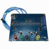
CDB5534U
Description
EVAL BOARD FOR CS5534
Manufacturer
Cirrus Logic Inc
Specifications of CDB5534U
Number Of Adc's
1
Number Of Bits
24
Sampling Rate (per Second)
3.84k
Data Interface
Serial
Inputs Per Adc
2 Single
Input Range
0 ~ 2.5 V
Power (typ) @ Conditions
35mW @ 5 V
Voltage Supply Source
Analog and Digital, Dual ±
Operating Temperature
-40°C ~ 85°C
Utilized Ic / Part
CS5534
Description/function
Audio DSPs
Operating Supply Voltage
5 V
Product
Audio Modules
For Use With/related Products
C8051F320
Lead Free Status / RoHS Status
Contains lead / RoHS non-compliant
Lead Free Status / RoHS Status
Lead free / RoHS Compliant, Contains lead / RoHS non-compliant
Other names
598-1016


rial port returns to the command mode, where it
waits for a new command to be issued. The single
conversion mode will take longer than conversions
performed in the continuous conversion mode. The
number of clock cycles a single conversion takes
for each Output Word Rate (OWR) setting is listed
in Table 1. The
clock ambiguity is due to internal synchronization
between the SCLK input and the oscillator.
Note:
2.6.2. Continuous Conversion Mode
Based on the information provided in the channel-
setup registers (CSRs), continuous conversions are
performed using the Setup register contents pointed
to by the conversion command. The command byte
includes a pointer address to the Setup register to
be used during the conversion. Once transmitted,
the serial port enters data mode where it waits until
a conversion is complete. After the conversion is
34
(WR3-WR0)
0000
0001
0010
0100
1000
1001
1010
0011
1011
1100
Table 1. Conversion Timing – Single Mode
In the single conversion mode, more than one
conversion is actually performed, but only the
final, fully settled result is output to the
conversion data register.
±
1318328 ± 8
2629048 ± 8
171448 ± 8
335288 ± 8
662968 ± 8
17848 ± 8
28088 ± 8
48568 ± 8
89528 ± 8
8 (FRS = 0) or
7592 ± 8
FRS = 0
Clock Cycles
±
1581994 ± 10
3154858 ± 10
205738 ± 10
402346 ± 10
795562 ± 10
107434 ± 10
21418 ± 10
33706 ± 10
58282 ± 10
9110 ± 10
10 (FRS = 1)
FRS = 1
done, SDO falls to logic 0. Forty SCLKs are then
needed to read the conversion. The first 8 SCLKs
are used to clear the SDO flag. The last 32 SCLKs
are needed to read the conversion result. If
‘00000000’ is provided to SDI during the first 8
SCLKs when the SDO flag is cleared, the converter
remains in this conversion mode and continues to
convert the selected channel using the same CSR
Setup. In continuous conversion mode, not every
conversion word needs to be read. The user needs
only to read the conversion words required for the
application as SDO rises and falls to indicate the
availability of new conversion data. Note that if a
conversion is not read before the next conversion
data becomes available, it will be lost and replaced
by the new conversion data. To exit this conversion
mode, the user must provide ‘11111111’ to the SDI
pin during the first 8 SCLKs after SDO falls. If the
user decides to exit, 32 SCLKs are required to
clock out the last conversion before the converter
returns to command mode. The number of clock
cycles a continuous conversion takes for each Out-
put Word Setting is listed in Table 2. The first con-
version from the part in continuous conversion
mode will be longer than the following conversions
due to start-up overhead. The
(FRS = 1) clock ambiguity is due to internal syn-
chronization between the SCLK input and the os-
cillator.
Note:
When changing channels, or after performing
calibrations and/or single conversions, the
user must ignore the first three (for OWRs
less than 3200 Sps, MCLK = 4.9152 MHz) or
first five (for OWR ≥ 3200 Sps) conversions in
continuous conversion mode, as residual
filter coefficients must be flushed from the
filter before accurate conversions are
performed.
CS5531/32/33/34-AS
±
8 (FRS = 0) or
DS289F5
±
10
Related parts for CDB5534U
Image
Part Number
Description
Manufacturer
Datasheet
Request
R

Part Number:
Description:
Development Kit
Manufacturer:
Cirrus Logic Inc
Datasheet:
Part Number:
Description:
Development Kit
Manufacturer:
Cirrus Logic Inc
Datasheet:


Part Number:
Description:
High-efficiency PFC + Fluorescent Lamp Driver Reference Design
Manufacturer:
Cirrus Logic Inc
Datasheet:
Part Number:
Description:
Development Kit
Manufacturer:
Cirrus Logic Inc
Datasheet:
Part Number:
Description:
Development Kit
Manufacturer:
Cirrus Logic Inc
Datasheet:

Part Number:
Description:
Development Kit
Manufacturer:
Cirrus Logic Inc
Datasheet:
Part Number:
Description:
Development Kit
Manufacturer:
Cirrus Logic Inc
Datasheet:
Part Number:
Description:
Development Kit
Manufacturer:
Cirrus Logic Inc
Datasheet:
Part Number:
Description:
Development Kit
Manufacturer:
Cirrus Logic Inc
Datasheet:

Part Number:
Description:
EVALUATION BOARD FOR CS8427
Manufacturer:
Cirrus Logic Inc
Datasheet:

Part Number:
Description:
BOARD EVAL FOR CS8416 RCVR
Manufacturer:
Cirrus Logic Inc
Datasheet:

Part Number:
Description:
EVALUATION BOARD FOR CS8420
Manufacturer:
Cirrus Logic Inc
Datasheet:

Part Number:
Description:
KIT DEVELOPMENT EP9315 ARM9
Manufacturer:
Cirrus Logic Inc
Datasheet:

Part Number:
Description:
KIT DEVELOPMENT EP9302 ARM9
Manufacturer:
Cirrus Logic Inc
Datasheet: