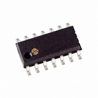
PIC16F630-I/SL Microchip Technology, PIC16F630-I/SL Datasheet - Page 46

PIC16F630-I/SL
Manufacturer Part Number
PIC16F630-I/SL
Description
IC MCU FLASH 1KX14 EEPROM 14SOIC
Manufacturer
Microchip Technology
Series
PIC® 16Fr
Datasheets
1.PIC16F616T-ISL.pdf
(8 pages)
2.PIC12F629T-ISN.pdf
(24 pages)
3.PIC16F630-ISL.pdf
(132 pages)
4.PIC16F630-ISL.pdf
(2 pages)
5.PIC16F630-ISL.pdf
(10 pages)
6.PIC16F676-EP.pdf
(132 pages)
7.PIC16F676-ISL.pdf
(130 pages)
Specifications of PIC16F630-I/SL
Program Memory Type
FLASH
Program Memory Size
1.75KB (1K x 14)
Package / Case
14-SOIC (3.9mm Width), 14-SOL
Core Processor
PIC
Core Size
8-Bit
Speed
20MHz
Peripherals
Brown-out Detect/Reset, POR, WDT
Number Of I /o
12
Eeprom Size
128 x 8
Ram Size
64 x 8
Voltage - Supply (vcc/vdd)
2 V ~ 5.5 V
Oscillator Type
Internal
Operating Temperature
-40°C ~ 85°C
Processor Series
PIC16F
Core
PIC
Data Bus Width
8 bit
Data Ram Size
64 B
Interface Type
RS- 232/USB
Maximum Clock Frequency
20 MHz
Number Of Programmable I/os
12
Number Of Timers
2
Operating Supply Voltage
2 V to 5.5 V
Maximum Operating Temperature
+ 85 C
Mounting Style
SMD/SMT
3rd Party Development Tools
52715-96, 52716-328, 52717-734
Development Tools By Supplier
PG164130, DV164035, DV244005, DV164005, PG164120, ICE2000, DM163014, DM164120-4
Minimum Operating Temperature
- 40 C
Package
14SOIC N
Device Core
PIC
Family Name
PIC16
Maximum Speed
20 MHz
Lead Free Status / RoHS Status
Lead free / RoHS Compliant
Data Converters
-
Connectivity
-
Lead Free Status / Rohs Status
Lead free / RoHS Compliant
Available stocks
Company
Part Number
Manufacturer
Quantity
Price
Company:
Part Number:
PIC16F630-I/SL
Manufacturer:
TriQuint
Quantity:
1 200
Company:
Part Number:
PIC16F630-I/SL
Manufacturer:
MICROCHI
Quantity:
1 743
Part Number:
PIC16F630-I/SL
Manufacturer:
MICROCHIP/微芯
Quantity:
20 000
PIC16F630/676
TABLE 7-1:
7.1.5
The A/D conversion is initiated by setting the
GO/DONE bit (ADCON0<1>). When the conversion is
complete, the A/D module:
• Clears the GO/DONE bit
• Sets the ADIF flag (PIR1<6>)
• Generates an interrupt (if enabled)
If the conversion must be aborted, the GO/DONE bit
can be cleared in software. The ADRESH:ADRESL
registers will not be updated with the partially complete
A/D
ADRESH:ADRESL registers will retain the value of the
FIGURE 7-2:
DS40039E-page 44
Legend: Shaded cells are outside of recommended range.
Note 1: The A/D RC source has a typical T
Operation
16 T
32 T
64 T
(ADFM = 0)
(ADFM = 1)
A/D RC
2 T
4 T
8 T
A/D Clock Source (T
2: These values violate the minimum required T
3: For faster conversion times, the selection of another clock source is recommended.
4: When the device frequency is greater than 1 MHz, the A/D RC clock source is only recommended if the
OSC
OSC
OSC
OSC
OSC
OSC
conversion
conversion will be performed during SLEEP.
STARTING A CONVERSION
ADCS2:ADCS0
T
AD
MSB
10-BIT A/D RESULT FORMAT
bit 7
bit 7
vs. DEVICE OPERATING FREQUENCIES
000
100
001
101
010
110
x11
sample.
Unimplemented: Read as ‘0
AD
)
Instead,
ADRESH
2 - 6 μs
100 ns
200 ns
400 ns
800 ns
20 MHz
1.6 μs
3.2 μs
10-bit A/D Result
AD
(1,4)
time of 4 μs for V
(2)
(2)
(2)
(2)
the
MSB
AD
time.
bit 0
bit 0
2 - 6 μs
12.8 μs
400 ns
800 ns
previous conversion. After an aborted conversion, a
2 T
be initiated. Following the delay, an input acquisition is
automatically started on the selected channel.
7.1.6
The A/D conversion can be supplied in two formats: left
or right shifted. The ADFM bit (ADCON0<7>) controls
the output format. Figure 7-2 shows the output formats.
5 MHz
1.6 μs
3.2 μs
6.4 μs
DD
Note:
AD
Device Frequency
> 3.0V.
(1,4)
(2)
(2)
(3)
delay is required before another acquisition can
bit 7
bit 7
The GO/DONE bit should not be set in the
same instruction that turns on the A/D.
CONVERSION OUTPUT
10-bit A/D Result
LSB
2 - 6 μs
16.0 μs
500 ns
1.0 μs
8.0 μs
4 MHz
2.0 μs
4.0 μs
Unimplemented: Read as ‘0’
© 2007 Microchip Technology Inc.
ADRESL
(2)
(3)
(1,4)
(2)
(3)
2 - 6 μs
1.25 MHz
12.8 μs
25.6 μs
51.2 μs
1.6 μs
3.2 μs
6.4 μs
bit 0
LSB
bit 0
(1,4)
(3)
(3)
(3)


