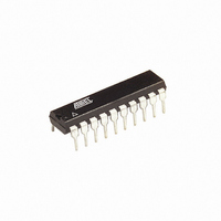
AT89LP2052-20PU Atmel, AT89LP2052-20PU Datasheet - Page 41

AT89LP2052-20PU
Manufacturer Part Number
AT89LP2052-20PU
Description
IC 8051 MCU FLASH 2K 20DIP
Manufacturer
Atmel
Series
89LPr
Datasheet
1.AT89LP2052-20PU.pdf
(94 pages)
Specifications of AT89LP2052-20PU
Core Processor
8051
Core Size
8-Bit
Speed
20MHz
Connectivity
SPI, UART/USART
Peripherals
Brown-out Detect/Reset, POR, PWM, WDT
Number Of I /o
15
Program Memory Size
2KB (2K x 8)
Program Memory Type
FLASH
Ram Size
256 x 8
Voltage - Supply (vcc/vdd)
2.4 V ~ 5.5 V
Oscillator Type
Internal
Operating Temperature
-40°C ~ 85°C
Package / Case
20-DIP (0.300", 7.62mm)
Processor Series
AT89x
Core
8051
Data Bus Width
8 bit
Data Ram Size
256 B
Interface Type
SPI/UART
Maximum Clock Frequency
20 MHz
Number Of Programmable I/os
15
Number Of Timers
2
Operating Supply Voltage
2.4 V to 5.5 V
Maximum Operating Temperature
+ 85 C
Mounting Style
Through Hole
3rd Party Development Tools
PK51, CA51, A51, ULINK2
Development Tools By Supplier
AT89ISP
Minimum Operating Temperature
- 40 C
Package
20PDIP
Device Core
8051
Family Name
AT89
Maximum Speed
20 MHz
Cpu Family
AT89
Device Core Size
8b
Frequency (max)
20MHz
Total Internal Ram Size
256Byte
# I/os (max)
15
Number Of Timers - General Purpose
2
Operating Supply Voltage (typ)
2.5/3.3/5V
Operating Supply Voltage (max)
5.5V
Operating Supply Voltage (min)
2.4V
Instruction Set Architecture
CISC
Operating Temp Range
-40C to 85C
Operating Temperature Classification
Industrial
Mounting
Through Hole
Pin Count
20
Package Type
PDIP
Lead Free Status / RoHS Status
Lead free / RoHS Compliant
Eeprom Size
-
Data Converters
-
Lead Free Status / Rohs Status
Lead free / RoHS Compliant
Available stocks
Company
Part Number
Manufacturer
Quantity
Price
Company:
Part Number:
AT89LP2052-20PU
Manufacturer:
ON
Quantity:
340
18.6
18.7
3547J–MICRO–10/09
Framing Error Detection
Automatic Address Recognition
When used for framing error detect, the UART looks for missing stop bits in the communication.
A missing bit will set the FE bit in the SCON register. The FE bit shares the SCON.7 bit with SM0
and the function of SCON.7 is determined by PCON.6 (SMOD0). If SMOD0 is set then SCON.7
functions as FE. SCON.7 functions as SM0 when SMOD0 is cleared. When used as FE,
SCON.7 can only be cleared by software.
Automatic Address Recognition is a feature which allows the UART to recognize certain
addresses in the serial bit stream by using hardware to make the comparisons. This feature
saves a great deal of software overhead by eliminating the need for the software to examine
every serial address which passes by the serial port. This feature is enabled by setting the SM2
bit in SCON. In the 9-bit UART modes, Mode 2 and Mode 3, the Receive Interrupt flag (RI) will
be automatically set when the received byte contains either the “Given” address or the “Broad-
cast” address. The 9-bit mode requires that the 9th information bit is a “1” to indicate that the
received information is an address and not data.
The 8-bit mode is called Mode 1. In this mode the RI flag will be set if SM2 is enabled and the
information received has a valid stop bit following the 8 address bits and the information is either
a Given or Broadcast address.
Mode 0 is the Shift Register mode and SM2 is ignored.
Using the Automatic Address Recognition feature allows a master to selectively communicate
with one or more slaves by invoking the given slave address or addresses. All of the slaves may
be contacted by using the Broadcast address. Two special Function Registers are used to
define the slave’s address, SADDR, and the address mask, SADEN. SADEN is used to define
which bits in the SADDR are to be used and which bits are “don’t care”. The SADEN mask can
be logically ANDed with the SADDR to create the “Given” address which the master will use for
addressing each of the slaves. Use of the Given address allows multiple slaves to be recognized
while excluding others. The following examples will help to show the versatility of this scheme:
Slave 0
Slave 1
In the previous example SADDR is the same and the SADEN data is used to differentiate
between the two slaves. Slave 0 requires a “0” in bit 0 and it ignores bit 1. Slave 1 requires a “0”
in bit 1 and bit 0 is ignored. A unique address for slave 0 would be 1100 0010 since slave 1
requires a “0” in bit 1. A unique address for slave 1 would be 1100 0001 since a “1” in bit 0 will
exclude slave 0. Both slaves can be selected at the same time by an address which has bit 0 = 0
(for slave 0) and bit 1 = 0 (for slave 1). Thus, both could be addressed with 1100 0000.
SADDR = 1100 0000
SADEN = 1111 1101
Given = 1100 00X0
SADDR = 1100 0000
SADEN = 1111 1110
Given = 1100 000X
AT89LP2052/LP4052
41


