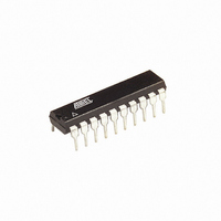
AT89LP2052-20PU Atmel, AT89LP2052-20PU Datasheet - Page 83

AT89LP2052-20PU
Manufacturer Part Number
AT89LP2052-20PU
Description
IC 8051 MCU FLASH 2K 20DIP
Manufacturer
Atmel
Series
89LPr
Datasheet
1.AT89LP2052-20PU.pdf
(94 pages)
Specifications of AT89LP2052-20PU
Core Processor
8051
Core Size
8-Bit
Speed
20MHz
Connectivity
SPI, UART/USART
Peripherals
Brown-out Detect/Reset, POR, PWM, WDT
Number Of I /o
15
Program Memory Size
2KB (2K x 8)
Program Memory Type
FLASH
Ram Size
256 x 8
Voltage - Supply (vcc/vdd)
2.4 V ~ 5.5 V
Oscillator Type
Internal
Operating Temperature
-40°C ~ 85°C
Package / Case
20-DIP (0.300", 7.62mm)
Processor Series
AT89x
Core
8051
Data Bus Width
8 bit
Data Ram Size
256 B
Interface Type
SPI/UART
Maximum Clock Frequency
20 MHz
Number Of Programmable I/os
15
Number Of Timers
2
Operating Supply Voltage
2.4 V to 5.5 V
Maximum Operating Temperature
+ 85 C
Mounting Style
Through Hole
3rd Party Development Tools
PK51, CA51, A51, ULINK2
Development Tools By Supplier
AT89ISP
Minimum Operating Temperature
- 40 C
Package
20PDIP
Device Core
8051
Family Name
AT89
Maximum Speed
20 MHz
Cpu Family
AT89
Device Core Size
8b
Frequency (max)
20MHz
Total Internal Ram Size
256Byte
# I/os (max)
15
Number Of Timers - General Purpose
2
Operating Supply Voltage (typ)
2.5/3.3/5V
Operating Supply Voltage (max)
5.5V
Operating Supply Voltage (min)
2.4V
Instruction Set Architecture
CISC
Operating Temp Range
-40C to 85C
Operating Temperature Classification
Industrial
Mounting
Through Hole
Pin Count
20
Package Type
PDIP
Lead Free Status / RoHS Status
Lead free / RoHS Compliant
Eeprom Size
-
Data Converters
-
Lead Free Status / Rohs Status
Lead free / RoHS Compliant
Available stocks
Company
Part Number
Manufacturer
Quantity
Price
Company:
Part Number:
AT89LP2052-20PU
Manufacturer:
ON
Quantity:
340
24.5
Table 24-4.
Note:
Figure 24-6. Shift Register Mode Timing Waveforms
24.6
24.6.1
Note:
24.6.2
Note:
3547J–MICRO–10/09
Symbol
t
t
t
t
t
XLXL
QVXH
XHQX
XHDX
XHDV
Serial Port Timing: Shift Register Mode
1. The values in this table are valid for V
Test Conditions
1. AC Inputs during testing are driven at V
1. For timing purposes, a port pin is no longer floating when a 100 mV change from load voltage occurs. A port pin begins to
WRITE TO SBUF
OUTPUT DATA
AC Testing Input/Output Waveforms
Float Waveforms
INPUT DATA
V
float when 100 mV change from the loaded V
CLEAR RI
Parameter
Serial Port Clock Cycle Time
Output Data Setup to Clock Rising Edge
Output Data Hold after Clock Rising Edge
Input Data Hold after Clock Rising Edge
Input Data Valid to Clock Rising Edge
IH
min. for a logic “1” and V
Serial Port Shift Register Timing Parameters
CLOCK
(1)
VALID
0
IL
max. for a logic “0”.
VALID
CC
1
CC
= 2.4V to 5.5V and Load Capacitance = 80 pF.
(1)
- 0.5V for a logic “1” and 0.45V for a logic “0”. Timing measurements are made at
OH
VALID
/V
OL
2
level occurs.
(1)
VALID
3
VALID
4
AT89LP2052/LP4052
2t
VALID
t
t
CLCL
CLCL
CLCL
Min
5
15
Variable Oscillator
0
-15
-15
-15
VALID
6
Max
VALID
7
Units
µs
ns
ns
ns
ns
83


