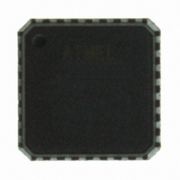
ATTINY48-MU Atmel, ATTINY48-MU Datasheet - Page 130

ATTINY48-MU
Manufacturer Part Number
ATTINY48-MU
Description
MCU AVR 4K ISP FLASH 1.8V 32-QFN
Manufacturer
Atmel
Series
AVR® ATtinyr
Specifications of ATTINY48-MU
Core Processor
AVR
Core Size
8-Bit
Speed
12MHz
Connectivity
I²C, SPI
Peripherals
Brown-out Detect/Reset, POR, WDT
Number Of I /o
28
Program Memory Size
4KB (2K x 16)
Program Memory Type
FLASH
Eeprom Size
64 x 8
Ram Size
256 x 8
Voltage - Supply (vcc/vdd)
1.8 V ~ 5.5 V
Data Converters
A/D 8x10b
Oscillator Type
Internal
Operating Temperature
-40°C ~ 85°C
Package / Case
32-VQFN Exposed Pad, 32-HVQFN, 32-SQFN, 32-DHVQFN
Processor Series
ATTINY4x
Core
AVR8
Data Bus Width
8 bit
Data Ram Size
256 B
Interface Type
2-Wire, I2S, SPI
Maximum Clock Frequency
12 MHz
Number Of Programmable I/os
24
Number Of Timers
2
Maximum Operating Temperature
+ 85 C
Mounting Style
SMD/SMT
3rd Party Development Tools
EWAVR, EWAVR-BL
Development Tools By Supplier
ATAVRDRAGON, ATSTK500, ATSTK600, ATAVRISP2, ATAVRONEKIT
Minimum Operating Temperature
- 40 C
On-chip Adc
10 bit, 8 Channel
Package
32QFN EP
Device Core
AVR
Family Name
ATtiny
Maximum Speed
12 MHz
Operating Supply Voltage
2.5|3.3|5 V
For Use With
ATSTK600 - DEV KIT FOR AVR/AVR32ATAVRDRAGON - KIT DRAGON 32KB FLASH MEM AVRATAVRISP2 - PROGRAMMER AVR IN SYSTEM
Lead Free Status / RoHS Status
Lead free / RoHS Compliant
Available stocks
Company
Part Number
Manufacturer
Quantity
Price
Company:
Part Number:
ATTINY48-MU
Manufacturer:
Atmel
Quantity:
5
Company:
Part Number:
ATTINY48-MU
Manufacturer:
LT
Quantity:
416
Part Number:
ATTINY48-MU
Manufacturer:
ATMEL/爱特梅尔
Quantity:
20 000
Part Number:
ATTINY48-MUR
Manufacturer:
ATMEL/爱特梅尔
Quantity:
20 000
- Current page: 130 of 302
- Download datasheet (9Mb)
15.3.1
15.3.2
15.4
15.4.1
130
Data Transfer and Frame Format
ATtiny48/88
TWI Terminology
Electrical Interconnection
Transferring Bits
The following definitions are frequently encountered in this section.
Table 15-1.
The PRTWI bit in
enable the 2-wire Serial Interface.
As depicted in
pull-up resistors. The bus drivers of all TWI-compliant devices are open-drain or open-collector.
This implements a wired-AND function which is essential to the operation of the interface. A low
level on a TWI bus line is generated when one or more TWI devices output a zero. A high level
is output when all TWI devices tri-state their outputs, allowing the pull-up resistors to pull the line
high. Note that all AVR devices connected to the TWI bus must be powered in order to allow any
bus operation.
The number of devices that can be connected to the bus is only limited by the bus capacitance
limit of 400 pF and the 7-bit slave address space. A detailed specification of the electrical char-
acteristics of the TWI is given in
different sets of specifications are presented there, one relevant for bus speeds below 100 kHz,
and one valid for bus speeds up to 400 kHz.
Each data bit transferred on the TWI bus is accompanied by a pulse on the clock line. The level
of the data line must be stable when the clock line is high. The only exception to this rule is for
generating start and stop conditions.
Figure 15-2. Data Validity
Term
Master
Slave
Transmitter
Receiver
SDA
SCL
TWI Terminology
Figure
Description
The device that initiates and terminates a transmission and generates the SCL clock.
The device addressed by a Master.
The device placing data on the bus.
The device reading data from the bus.
“PRR – Power Reduction Register” on page 40
15-1, both bus lines are connected to the positive supply voltage through
Data Stable
“Two-Wire Serial Interface Characteristics” on page
Data Change
Data Stable
must be written to zero to
8008G–AVR–04/11
212. Two
Related parts for ATTINY48-MU
Image
Part Number
Description
Manufacturer
Datasheet
Request
R

Part Number:
Description:
Manufacturer:
Atmel Corporation
Datasheet:

Part Number:
Description:
Microcontrollers (MCU) 512B FL 32B SRAM TIMER ATTINY4 12MHz
Manufacturer:
Atmel

Part Number:
Description:
IC MCU AVR 512B FLASH SOT-23-6
Manufacturer:
Atmel
Datasheet:

Part Number:
Description:
IC MCU AVR 512B FLASH SOT-23-6
Manufacturer:
Atmel
Datasheet:

Part Number:
Description:
IC, MCU, 8BIT, 2K FLASH, 20SOIC
Manufacturer:
Atmel
Datasheet:

Part Number:
Description:
IC, MCU, 8BIT, 2K FLASH, 20PDIP
Manufacturer:
Atmel
Datasheet:

Part Number:
Description:
IC, MCU, 8BIT, 8K FLASH, 20PDIP
Manufacturer:
Atmel
Datasheet:

Part Number:
Description:
IC, MCU, 8BIT, 8K FLASH, 20SOIC
Manufacturer:
Atmel
Datasheet:

Part Number:
Description:
DEV KIT FOR AVR/AVR32
Manufacturer:
Atmel
Datasheet:

Part Number:
Description:
INTERVAL AND WIPE/WASH WIPER CONTROL IC WITH DELAY
Manufacturer:
ATMEL Corporation
Datasheet:

Part Number:
Description:
Low-Voltage Voice-Switched IC for Hands-Free Operation
Manufacturer:
ATMEL Corporation
Datasheet:

Part Number:
Description:
MONOLITHIC INTEGRATED FEATUREPHONE CIRCUIT
Manufacturer:
ATMEL Corporation
Datasheet:

Part Number:
Description:
AM-FM Receiver IC U4255BM-M
Manufacturer:
ATMEL Corporation
Datasheet:


