ATTINY48-MU Atmel, ATTINY48-MU Datasheet - Page 32
ATTINY48-MU
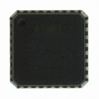
Manufacturer Part Number
ATTINY48-MU
Description
MCU AVR 4K ISP FLASH 1.8V 32-QFN
Manufacturer
Atmel
Series
AVR® ATtinyr
Specifications of ATTINY48-MU
Core Processor
AVR
Core Size
8-Bit
Speed
12MHz
Connectivity
I²C, SPI
Peripherals
Brown-out Detect/Reset, POR, WDT
Number Of I /o
28
Program Memory Size
4KB (2K x 16)
Program Memory Type
FLASH
Eeprom Size
64 x 8
Ram Size
256 x 8
Voltage - Supply (vcc/vdd)
1.8 V ~ 5.5 V
Data Converters
A/D 8x10b
Oscillator Type
Internal
Operating Temperature
-40°C ~ 85°C
Package / Case
32-VQFN Exposed Pad, 32-HVQFN, 32-SQFN, 32-DHVQFN
Processor Series
ATTINY4x
Core
AVR8
Data Bus Width
8 bit
Data Ram Size
256 B
Interface Type
2-Wire, I2S, SPI
Maximum Clock Frequency
12 MHz
Number Of Programmable I/os
24
Number Of Timers
2
Maximum Operating Temperature
+ 85 C
Mounting Style
SMD/SMT
3rd Party Development Tools
EWAVR, EWAVR-BL
Development Tools By Supplier
ATAVRDRAGON, ATSTK500, ATSTK600, ATAVRISP2, ATAVRONEKIT
Minimum Operating Temperature
- 40 C
On-chip Adc
10 bit, 8 Channel
Package
32QFN EP
Device Core
AVR
Family Name
ATtiny
Maximum Speed
12 MHz
Operating Supply Voltage
2.5|3.3|5 V
For Use With
ATSTK600 - DEV KIT FOR AVR/AVR32ATAVRDRAGON - KIT DRAGON 32KB FLASH MEM AVRATAVRISP2 - PROGRAMMER AVR IN SYSTEM
Lead Free Status / RoHS Status
Lead free / RoHS Compliant
Available stocks
Company
Part Number
Manufacturer
Quantity
Price
Company:

Part Number:
ATTINY48-MU
Manufacturer:
Atmel
Quantity:
5
Company:
Part Number:
ATTINY48-MU
Manufacturer:
LT
Quantity:
416
Part Number:
ATTINY48-MU
Manufacturer:
ATMEL/爱特梅尔
Quantity:
20 000
Part Number:
ATTINY48-MUR
Manufacturer:
ATMEL/爱特梅尔
Quantity:
20 000


6.3.1
6.4
6.5
32
Clock Output Buffer
Clock Startup Sequence
ATtiny48/88
Switching Prescaler Setting
is low. This can be used with all clock source options, and it will affect the clock frequency of the
CPU and all synchronous peripherals. clk
as shown in
When switching between prescaler settings, the System Clock Prescaler ensures that no
glitches occur in the clock system. It also ensures that no intermediate frequency is higher than
neither the clock frequency corresponding to the previous setting, nor the clock frequency corre-
sponding to the new setting.
The ripple counter that implements the prescaler runs at the frequency of the undivided clock,
which may be faster than the CPU's clock frequency. Hence, it is not possible to determine the
state of the prescaler – even if it were readable, and the exact time it takes to switch from one
clock division to the other cannot be exactly predicted.
From the time the CLKPS values are written, it takes between T1 + T2 and T1 + 2 * T2 before
the new clock frequency is active. In this interval, 2 active clock edges are produced. Here, T1 is
the previous clock period, and T2 is the period corresponding to the new prescaler setting.
To avoid unintentional changes of clock frequency, a special write procedure must befollowed to
change the CLKPS bits:
Interrupts must be disabled when changing prescaler setting to make sure the write procedure is
not interrupted.
The device can output the system clock on the CLKO pin. To enable the output, the CKOUT
Fuse has to be programmed. This mode is suitable when the chip clock is used to drive other cir-
cuits on the system. The clock also will be output during reset, and the normal operation of I/O
pin will be overridden when the fuse is programmed. Any clock source, including the internal
oscillator, can be selected when the clock is output on CLKO. If the System Clock Prescaler is
used, it is the divided system clock that is output.
Any clock source needs a sufficient V
cycles before it can be considered stable.
To ensure sufficient V
the device reset is released by all other reset sources.
describes the start conditions for the internal reset. The delay (t
oscillator and the number of cycles in the delay is set by the SUTx and CKSELx fuse bits. The
selectable delays are shown in
1. Write the Clock Prescaler Change Enable (CLKPCE) bit to one and all other bitsin
2. Within four cycles, write the desired value to CLKPS while writing a zero to CLKPCE.
CLKPR to zero.
Table 6-6 on page
CC
, the device issues an internal reset with a time-out delay (t
35.
Table
CC
6-5. The frequency of the Watchdog oscillator is voltage
to start oscillating and a minimum number of oscillating
I/O
, clk
ADC
, clk
CPU
“System Control and Reset” on page 42
, and clk
TOUT
) is timed from the Watchdog
FLASH
are divided by a factor
8008G–AVR–04/11
TOUT
) after
Related parts for ATTINY48-MU
Image
Part Number
Description
Manufacturer
Datasheet
Request
R

Part Number:
Description:
Manufacturer:
Atmel Corporation
Datasheet:

Part Number:
Description:
Microcontrollers (MCU) 512B FL 32B SRAM TIMER ATTINY4 12MHz
Manufacturer:
Atmel
Part Number:
Description:
IC MCU AVR 512B FLASH SOT-23-6
Manufacturer:
Atmel
Datasheet:

Part Number:
Description:
IC MCU AVR 512B FLASH SOT-23-6
Manufacturer:
Atmel
Datasheet:
Part Number:
Description:
IC, MCU, 8BIT, 2K FLASH, 20SOIC
Manufacturer:
Atmel
Datasheet:

Part Number:
Description:
IC, MCU, 8BIT, 2K FLASH, 20PDIP
Manufacturer:
Atmel
Datasheet:
Part Number:
Description:
IC, MCU, 8BIT, 8K FLASH, 20PDIP
Manufacturer:
Atmel
Datasheet:
Part Number:
Description:
IC, MCU, 8BIT, 8K FLASH, 20SOIC
Manufacturer:
Atmel
Datasheet:

Part Number:
Description:
DEV KIT FOR AVR/AVR32
Manufacturer:
Atmel
Datasheet:
Part Number:
Description:
INTERVAL AND WIPE/WASH WIPER CONTROL IC WITH DELAY
Manufacturer:
ATMEL Corporation
Datasheet:
Part Number:
Description:
Low-Voltage Voice-Switched IC for Hands-Free Operation
Manufacturer:
ATMEL Corporation
Datasheet:
Part Number:
Description:
MONOLITHIC INTEGRATED FEATUREPHONE CIRCUIT
Manufacturer:
ATMEL Corporation
Datasheet:
Part Number:
Description:
AM-FM Receiver IC U4255BM-M
Manufacturer:
ATMEL Corporation
Datasheet: