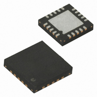
ATTINY2313V-10MU Atmel, ATTINY2313V-10MU Datasheet - Page 144

ATTINY2313V-10MU
Manufacturer Part Number
ATTINY2313V-10MU
Description
10MHZ MLF IND TEMP GREEN
Manufacturer
Atmel
Series
AVR® ATtinyr
Datasheets
1.ATTINY2313-20MU.pdf
(226 pages)
2.ATTINY2313V-10MU.pdf
(15 pages)
3.ATTINY2313V-10SU.pdf
(20 pages)
Specifications of ATTINY2313V-10MU
Core Processor
AVR
Core Size
8-Bit
Speed
10MHz
Connectivity
SPI, UART/USART
Peripherals
Brown-out Detect/Reset, POR, PWM, WDT
Number Of I /o
18
Program Memory Size
2KB (1K x 16)
Program Memory Type
FLASH
Eeprom Size
128 x 8
Ram Size
128 x 8
Voltage - Supply (vcc/vdd)
1.8 V ~ 5.5 V
Oscillator Type
Internal
Operating Temperature
-40°C ~ 85°C
Package / Case
20-MLF®, QFN
Processor Series
ATTINY2x
Core
AVR8
Data Bus Width
8 bit
Data Ram Size
128 B
Interface Type
SPI/UART/USI
Maximum Clock Frequency
10 MHz
Number Of Programmable I/os
18
Number Of Timers
2
Operating Supply Voltage
1.8 V to 5.5 V
Maximum Operating Temperature
+ 85 C
Mounting Style
SMD/SMT
Minimum Operating Temperature
- 40 C
For Use With
ATSTK600-DIP40 - STK600 SOCKET/ADAPTER 40-PDIP770-1007 - ISP 4PORT ATMEL AVR MCU SPI/JTAGATAVRDRAGON - KIT DRAGON 32KB FLASH MEM AVRATAVRISP2 - PROGRAMMER AVR IN SYSTEMATJTAGICE2 - AVR ON-CHIP D-BUG SYSTEM
Lead Free Status / RoHS Status
Lead free / RoHS Compliant
Data Converters
-
Lead Free Status / Rohs Status
Lead free / RoHS Compliant
Other names
Q2312268B
Available stocks
Company
Part Number
Manufacturer
Quantity
Price
Part Number:
ATTINY2313V-10MU
Manufacturer:
ATMEL/爱特梅尔
Quantity:
20 000
Start Condition
Detector
Alternative USI
Usage
Half-duplex
Asynchronous Data
Transfer
4-bit Counter
12-bit Timer/Counter
Edge Triggered
External Interrupt
Software Interrupt
USI Register
Descriptions
USI Data Register –
USIDR
144
ATtiny2313
The start condition detector is shown in Figure 65. The SDA line is delayed (in the range of 50 to
300 ns) to ensure valid sampling of the SCL line.
The start condition detector is working asynchronously and can therefore wake up the processor
from the Power-down sleep mode. However, the protocol used might have restrictions on the
SCL hold time. Therefore, when using this feature in this case the Oscillator start-up time set by
the CKSEL Fuses (see
into the consideration.
When the USI unit is not used for serial communication, it can be set up to do alternative tasks
due to its flexible design.
By utilizing the Shift Register in Three-wire mode, it is possible to implement a more compact
and higher performance UART than by software only.
The 4-bit counter can be used as a stand-alone counter with overflow interrupt. Note that if the
counter is clocked externally, both clock edges will generate an increment.
Combining the USI 4-bit counter and Timer/Counter0 allows them to be used as a 12-bit
counter.
By setting the counter to maximum value (F) it can function as an additional external interrupt.
The overflow flag and interrupt enable bit are then used for the external interrupt. This feature is
selected by the USICS1 bit.
The counter overflow interrupt can be used as a software interrupt triggered by a clock strobe.
The USI uses no buffering of the serial register, i.e., when accessing the Data Register (USIDR)
the serial register is accessed directly. If a serial clock occurs at the same cycle the register is
written, the register will contain the value written and no shift is performed. A (left) shift operation
is performed depending of the USICS1..0 bits setting. The shift operation can be controlled by
an external clock edge, by a Timer/Counter0 overflow, or directly by software using the USICLK
strobe bit. Note that even when no wire mode is selected (USIWM1..0 = 0) both the external
data input (DI/SDA) and the external clock input (USCK/SCL) can still be used by the Shift
Register.
The output pin in use, DO or SDA depending on the wire mode, is connected via the output latch
to the most significant bit (bit 7) of the Data Register. The output latch is open (transparent) dur-
ing the first half of a serial clock cycle when an external clock source is selected (USICS1 = 1),
and constantly open when an internal clock source is used (USICS1 = 0). The output will be
changed immediately when a new MSB written as long as the latch is open. The latch ensures
that data input is sampled and data output is changed on opposite clock edges.
Note that the corresponding Data Direction Register to the pin must be set to one for enabling
data output from the Shift Register.
Bit
Read/Write
Initial Value
MSB
R/W
7
0
R/W
“Clock Systems and their Distribution” on page
6
0
R/W
5
0
R/W
4
0
R/W
3
0
R/W
2
0
R/W
1
0
22) must also be taken
LSB
R/W
0
0
USIDR
2543L–AVR–08/10


