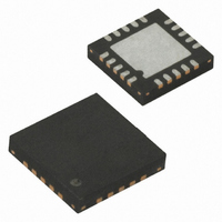
ATTINY2313V-10MU Atmel, ATTINY2313V-10MU Datasheet - Page 51

ATTINY2313V-10MU
Manufacturer Part Number
ATTINY2313V-10MU
Description
10MHZ MLF IND TEMP GREEN
Manufacturer
Atmel
Series
AVR® ATtinyr
Datasheets
1.ATTINY2313-20MU.pdf
(226 pages)
2.ATTINY2313V-10MU.pdf
(15 pages)
3.ATTINY2313V-10SU.pdf
(20 pages)
Specifications of ATTINY2313V-10MU
Core Processor
AVR
Core Size
8-Bit
Speed
10MHz
Connectivity
SPI, UART/USART
Peripherals
Brown-out Detect/Reset, POR, PWM, WDT
Number Of I /o
18
Program Memory Size
2KB (1K x 16)
Program Memory Type
FLASH
Eeprom Size
128 x 8
Ram Size
128 x 8
Voltage - Supply (vcc/vdd)
1.8 V ~ 5.5 V
Oscillator Type
Internal
Operating Temperature
-40°C ~ 85°C
Package / Case
20-MLF®, QFN
Processor Series
ATTINY2x
Core
AVR8
Data Bus Width
8 bit
Data Ram Size
128 B
Interface Type
SPI/UART/USI
Maximum Clock Frequency
10 MHz
Number Of Programmable I/os
18
Number Of Timers
2
Operating Supply Voltage
1.8 V to 5.5 V
Maximum Operating Temperature
+ 85 C
Mounting Style
SMD/SMT
Minimum Operating Temperature
- 40 C
For Use With
ATSTK600-DIP40 - STK600 SOCKET/ADAPTER 40-PDIP770-1007 - ISP 4PORT ATMEL AVR MCU SPI/JTAGATAVRDRAGON - KIT DRAGON 32KB FLASH MEM AVRATAVRISP2 - PROGRAMMER AVR IN SYSTEMATJTAGICE2 - AVR ON-CHIP D-BUG SYSTEM
Lead Free Status / RoHS Status
Lead free / RoHS Compliant
Data Converters
-
Lead Free Status / Rohs Status
Lead free / RoHS Compliant
Other names
Q2312268B
Available stocks
Company
Part Number
Manufacturer
Quantity
Price
Part Number:
ATTINY2313V-10MU
Manufacturer:
ATMEL/爱特梅尔
Quantity:
20 000
- Current page: 51 of 226
- Download datasheet (4Mb)
Alternate Port
Functions
2543L–AVR–08/10
Most port pins have alternate functions in addition to being general digital I/Os.
how the port pin control signals from the simplified
functions. The overriding signals may not be present in all port pins, but the figure serves as a
generic description applicable to all port pins in the AVR microcontroller family.
Figure 25. Alternate Port Functions
Note:
Table 23
ure 25
the modules having the alternate function.
PTOExn:
PUOExn:
PUOVxn:
DDOExn:
DDOVxn:
PVOExn:
PVOVxn:
DIEOExn: Pxn DIGITAL INPUT-ENABLE OVERRIDE ENABLE
DIEOVxn: Pxn DIGITAL INPUT-ENABLE OVERRIDE VALUE
SLEEP:
Pxn
are not shown in the succeeding tables. The overriding signals are generated internally in
1. WRx, WPx, WDx, RRx, RPx, and RDx are common to all pins within the same port. clk
summarizes the function of the overriding signals. The pin and port indexes from
SLEEP, and PUD are common to all ports. All other signals are unique for each pin.
Pxn, PORT TOGGLE OVERRIDE ENABLE
Pxn PULL-UP OVERRIDE ENABLE
Pxn PULL-UP OVERRIDE VALUE
Pxn DATA DIRECTION OVERRIDE ENABLE
Pxn DATA DIRECTION OVERRIDE VALUE
Pxn PORT VALUE OVERRIDE ENABLE
Pxn PORT VALUE OVERRIDE VALUE
SLEEP CONTROL
1
0
1
0
1
0
1
0
(1)
PUOExn
PUOVxn
DDOExn
DDOVxn
PVOExn
PVOVxn
DIEOExn
DIEOVxn
SLEEP
PUD:
WDx:
RDx:
RRx:
WRx:
RPx:
WPx:
clk
DIxn:
AIOxn:
SYNCHRONIZER
D
L
I/O
SET
CLR
:
Q
Q
Figure 22
PULLUP DISABLE
WRITE DDRx
READ DDRx
READ PORTx REGISTER
WRITE PORTx
READ PORTx PIN
I/O CLOCK
DIGITAL INPUT PIN n ON PORTx
ANALOG INPUT/OUTPUT PIN n ON PORTx
D
WRITE PINx
PINxn
CLR
Q
Q
RESET
RESET
PORTxn
Q
Q
Q
Q
DDxn
CLR
CLR
D
D
can be overridden by alternate
1
0
clk
PUD
WDx
RDx
RRx
DIxn
AIOxn
RPx
I/O
WRx
PTOExn
WPx
Figure 25
shows
Fig-
I/O
51
,
Related parts for ATTINY2313V-10MU
Image
Part Number
Description
Manufacturer
Datasheet
Request
R

Part Number:
Description:
IC MCU AVR 2K FLASH 20DIP
Manufacturer:
Atmel
Datasheet:

Part Number:
Description:
IC MCU AVR 2K FLASH 20SOIC
Manufacturer:
Atmel
Datasheet:

Part Number:
Description:
Manufacturer:
Atmel Corporation
Datasheet:

Part Number:
Description:
Manufacturer:
ATMEL Corporation
Datasheet:

Part Number:
Description:
IC MCU AVR 2K FLASH 20MLF
Manufacturer:
Atmel
Datasheet:

Part Number:
Description:
IC MCU AVR 2K FLASH 20DIP
Manufacturer:
Atmel
Datasheet:

Part Number:
Description:
IC MCU AVR 2K FLASH 20SOIC
Manufacturer:
Atmel
Datasheet:

Part Number:
Description:
IC MCU AVR 2K FLASH 20DIP
Manufacturer:
Atmel
Datasheet:

Part Number:
Description:
IC MCU AVR 2K FLASH 20SOIC
Manufacturer:
Atmel
Datasheet:

Part Number:
Description:
IC MCU AVR 2K FLASH 20SOIC
Manufacturer:
Atmel
Datasheet:

Part Number:
Description:
IC MCU AVR 2K FLASH 20WQFN
Manufacturer:
Atmel
Datasheet:

Part Number:
Description:
8-bit AVR Microcontroller with 2K Bytes In-System Programmable Flash
Manufacturer:
ATMEL Corporation
Datasheet:

Part Number:
Description:
Attiny2313 8-bit With 2k Bytes Of In-system Programmable Flash
Manufacturer:
ATMEL Corporation
Datasheet:


