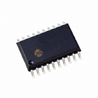
PIC18F13K50-I/SO Microchip Technology, PIC18F13K50-I/SO Datasheet - Page 27

PIC18F13K50-I/SO
Manufacturer Part Number
PIC18F13K50-I/SO
Description
IC PIC MCU FLASH 8K 1.8V 20-SOIC
Manufacturer
Microchip Technology
Series
PIC® XLP™ 18Fr
Datasheets
1.PIC18F13K50-ISS.pdf
(420 pages)
2.PIC18F13K50-ISS.pdf
(40 pages)
3.PIC18F13K50-ISS.pdf
(10 pages)
4.PIC18F13K50-ISS.pdf
(2 pages)
5.PIC18F13K50-ISO.pdf
(414 pages)
Specifications of PIC18F13K50-I/SO
Core Size
8-Bit
Program Memory Size
8KB (4K x 16)
Core Processor
PIC
Speed
48MHz
Connectivity
I²C, SPI, UART/USART, USB
Peripherals
Brown-out Detect/Reset, POR, PWM, WDT
Number Of I /o
14
Program Memory Type
FLASH
Eeprom Size
256 x 8
Ram Size
512 x 8
Voltage - Supply (vcc/vdd)
1.8 V ~ 5.5 V
Data Converters
A/D 11x10b
Oscillator Type
Internal
Operating Temperature
-40°C ~ 85°C
Package / Case
20-SOIC (7.5mm Width)
Controller Family/series
PIC18
No. Of I/o's
15
Eeprom Memory Size
256Byte
Ram Memory Size
512Byte
Cpu Speed
48MHz
No. Of Timers
4
Processor Series
PIC18F
Core
PIC
Data Bus Width
8 bit
Data Ram Size
512 B
Interface Type
EUSART, I2C, MSSP, SPI, USB
Maximum Clock Frequency
48 MHz
Number Of Programmable I/os
15
Number Of Timers
4
Maximum Operating Temperature
+ 85 C
Mounting Style
SMD/SMT
3rd Party Development Tools
52715-96, 52716-328, 52717-734, 52712-325, EWPIC18
Development Tools By Supplier
PG164130, DV164035, DV244005, DV164005, DM164127, DV164126
Minimum Operating Temperature
- 40 C
On-chip Adc
10 bit, 11 Channel
Package
20SOIC W
Device Core
PIC
Family Name
PIC18
Maximum Speed
48 MHz
Operating Supply Voltage
3.3|5 V
Lead Free Status / RoHS Status
Lead free / RoHS Compliant
For Use With
DV164126 - KIT DEVELOPMENT USB W/PICKIT 2DM164127 - KIT DEVELOPMENT USB 18F14/13K50AC164112 - VOLTAGE LIMITER MPLAB ICD2 VPPXLT20SO1-1 - SOCKET TRANS ICE 20DIP TO 20SOICAC164307 - MODULE SKT FOR PM3 28SSOP
Lead Free Status / Rohs Status
Details
Available stocks
Company
Part Number
Manufacturer
Quantity
Price
Part Number:
PIC18F13K50-I/SO
Manufacturer:
MICROCHIP/微芯
Quantity:
20 000
6.0
The PIC18F1XK50/PIC18LF1XK50 devices have
several Configuration Words. These bits can be set or
cleared to select various device configurations. All
other memory areas should be programmed and
verified prior to setting Configuration Words. These bits
may be read out normally, even after read or code
protection. See Table 6-1 for a list of Configuration bits
and device IDs, and Table 6-3 for the Configuration bit
descriptions.
6.1
A user may store identification information (ID) in eight
ID locations, mapped in 200000h:200007h. It is
recommended that the Most Significant nibble of each
ID be Fh. In doing so, if the user code inadvertently tries
to execute from the ID space, the ID data will execute
as a NOP.
TABLE 6-1:
2010 Microchip Technology Inc.
300000h
300001h
300002h
300003h
300005h
300006h
300008h
300009h
30000Ah
30000Bh
30000Ch
30000Dh
3FFFFEh
3FFFFFh
Legend:
Note
File Name
1:
2:
3:
CONFIGURATION WORD
ID Locations
CONFIG1L
CONFIG1H
CONFIG2L
CONFIG2H
CONFIG3H
CONFIG4L
CONFIG5L
CONFIG5H
CONFIG6L
CONFIG6H
CONFIG7L
CONFIG7H
DEVID1
DEVID2
x = unknown, u = unchanged, – = unimplemented. Shaded cells are unimplemented, read as ‘0’, q = conditional.
These bits are only implemented on specific devices. Refer to Section 3.0 “Memory Maps” to determine which bits apply based on
available memory.
DEVID registers are read-only and cannot be programmed by the user.
VREG is read-only. VREG = 1 for PIC18F1XK50 devices and VREG = 0 for PIC18LF1XK50 devices. The VREG bit value should not be
included in any Verify or Checksum operation.
(2)
(2)
CONFIGURATION BITS AND DEVICE IDs
MCLRE
DEV10
WRTD
DEV2
IESO
Bit 7
CPD
—
—
—
—
—
—
—
—
FCMEN
EBTRB
XINST
WRTB
DEV1
DEV9
Bit 6
CPB
—
—
—
—
—
—
—
PCLKEN
USBDIV
VREG
PIC18F1XK50/PIC18LF1XK50
WRTC
DEV0
DEV8
Bit 5
—
—
—
—
—
—
—
—
Advance Information
(3)
CPUDIV1
WDTPS3
BORV1
PLLEN
REV4
DEV7
Bit 4
—
—
—
—
—
—
—
—
6.2
The
PIC18LF1XK50
3FFFFEh:3FFFFFh. These bits may be used by the
programmer to identify what device type is being
programmed and read out normally, even after code or
read protection. See Table 6-2 for a complete list of
device ID values.
FIGURE 6-1:
CPUDIV0
WDTPS2
HFOFST
BORV0
FOSC3
BBSIZ
REV3
DEV6
Bit 3
—
—
—
—
—
—
device
Device ID Word
BOREN1
WDTPS1
FOSC2
REV2
DEV5
Bit 2
LVP
—
—
—
—
—
—
—
—
ID
Set TBLPTR = 3FFFFE
with Post-Increment
with Post-Increment
Read High Byte
Read Low Byte
word
devices
WDTPS0
BOREN0
FOSC1
EBTR1
WRT1
REV1
DEV4
READ DEVICE ID WORD
FLOW
Bit 1
CP1
—
—
—
—
—
—
Done
Start
for
PWRTEN
STVREN
WDTEN
FOSC0
EBTR0
WRT0
REV0
DEV3
Bit 0
CP0
the
is
—
—
—
—
—
DS41342E-page 27
PIC18F1XK50/
located
Unprogrammed
See Table 6-2
See Table 6-2
--00 0---
0010 0111
--q1 1111
---1 1111
1--- 1---
10-- 01-1
---- --11
11-- ----
---- --11
111- ----
---- --11
-1-- ----
Default/
Value
at


