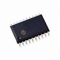
PIC18F13K50-I/SO Microchip Technology, PIC18F13K50-I/SO Datasheet - Page 35

PIC18F13K50-I/SO
Manufacturer Part Number
PIC18F13K50-I/SO
Description
IC PIC MCU FLASH 8K 1.8V 20-SOIC
Manufacturer
Microchip Technology
Series
PIC® XLP™ 18Fr
Datasheets
1.PIC18F13K50-ISS.pdf
(420 pages)
2.PIC18F13K50-ISS.pdf
(40 pages)
3.PIC18F13K50-ISS.pdf
(10 pages)
4.PIC18F13K50-ISS.pdf
(2 pages)
5.PIC18F13K50-ISO.pdf
(414 pages)
Specifications of PIC18F13K50-I/SO
Core Size
8-Bit
Program Memory Size
8KB (4K x 16)
Core Processor
PIC
Speed
48MHz
Connectivity
I²C, SPI, UART/USART, USB
Peripherals
Brown-out Detect/Reset, POR, PWM, WDT
Number Of I /o
14
Program Memory Type
FLASH
Eeprom Size
256 x 8
Ram Size
512 x 8
Voltage - Supply (vcc/vdd)
1.8 V ~ 5.5 V
Data Converters
A/D 11x10b
Oscillator Type
Internal
Operating Temperature
-40°C ~ 85°C
Package / Case
20-SOIC (7.5mm Width)
Controller Family/series
PIC18
No. Of I/o's
15
Eeprom Memory Size
256Byte
Ram Memory Size
512Byte
Cpu Speed
48MHz
No. Of Timers
4
Processor Series
PIC18F
Core
PIC
Data Bus Width
8 bit
Data Ram Size
512 B
Interface Type
EUSART, I2C, MSSP, SPI, USB
Maximum Clock Frequency
48 MHz
Number Of Programmable I/os
15
Number Of Timers
4
Maximum Operating Temperature
+ 85 C
Mounting Style
SMD/SMT
3rd Party Development Tools
52715-96, 52716-328, 52717-734, 52712-325, EWPIC18
Development Tools By Supplier
PG164130, DV164035, DV244005, DV164005, DM164127, DV164126
Minimum Operating Temperature
- 40 C
On-chip Adc
10 bit, 11 Channel
Package
20SOIC W
Device Core
PIC
Family Name
PIC18
Maximum Speed
48 MHz
Operating Supply Voltage
3.3|5 V
Lead Free Status / RoHS Status
Lead free / RoHS Compliant
For Use With
DV164126 - KIT DEVELOPMENT USB W/PICKIT 2DM164127 - KIT DEVELOPMENT USB 18F14/13K50AC164112 - VOLTAGE LIMITER MPLAB ICD2 VPPXLT20SO1-1 - SOCKET TRANS ICE 20DIP TO 20SOICAC164307 - MODULE SKT FOR PM3 28SSOP
Lead Free Status / Rohs Status
Details
Available stocks
Company
Part Number
Manufacturer
Quantity
Price
Part Number:
PIC18F13K50-I/SO
Manufacturer:
MICROCHIP/微芯
Quantity:
20 000
8.1
2010 Microchip Technology Inc.
Standard Operating Conditions
Operating Temperature: 25C is recommended
Param
D110
D110A V
D111
D112
D113
D031
D041
D042
D080
D090
D091
D012
P1
P2
P2A
P2B
P3
P4
P5
P5A
P6
P9
P9A
P10
P11
Note 1:
No.
V
V
I
I
V
V
V
V
V
V
C
T
T
T
T
T
T
T
T
T
T
T
T
T
PP
DDP
AC/DC Characteristics Timing Requirements for Program/Verify Test Mode
Sym.
DLY
IHH
IHL
DD
IL
IH
IH
OL
OH
OH
R
PGC
PGCL
PGCH
SET
HLD
DLY
DLY
DLY
DLY
DLY
DLY
IO
Do not allow excess time when transitioning MCLR between V
executions to occur. The maximum transition time is:
1 T
only) + 1.5 s (for EC mode only) where T
and T
data sheet for the particular device.
1
1
1
2
5
5
6
7
1
A
A
CY
High-Voltage Programming Voltage on
MCLR/V
Low-Voltage Programming Voltage on
MCLR/V
PIC18F1XK50 (includes Bulk Erase)
PIC18LF1XK50 (includes Bulk Erase)
Programming Current on MCLR/V
Supply Current During Programming
Input Low Voltage
Input High Voltage
Input High Voltage on RA0 and RA1 pins only
Output Low Voltage
Output High Voltage
Output High Voltage on RA0 pin only
Capacitive Loading on I/O pin (PGD)
MCLR/V
Program/Verify mode
Serial Clock (PGC) Period
Serial Clock (PGC) Low Time
Serial Clock (PGC) High Time
Input Data Setup Time to Serial Clock
Input Data Hold Time from PGC
Delay between 4-bit Command and Command
Operand
Delay between 4-bit Command Operand and next
4-bit Command
Delay between Last PGC of Command Byte to
First PGC of Read of Data Word
PGC High Time (minimum programming time)
PGC High Time
PGC Low Time after Programming
(high-voltage discharge time)
Delay to allow Self-Timed Data Write or
Bulk Erase to occur
OSC
+ T
PWRT
is the oscillator period. For specific values, refer to the Electrical Characteristics section of the device
PP
PP
PP
(if enabled) + 1024 T
/RA3
/RA3
/RA3 Rise Time to enter
Characteristic
PIC18F1XK50/PIC18LF1XK50
Advance Information
OSC
PP
(for LP, HS, HS/PLL and XT modes only) + 2 ms (for HS/PLL mode
/RA3
CY
is the instruction cycle time, T
V
V
0.8 V
0.8 V
USB
DD
Min.
1.80
2.70
2.70
V
M
100
400
400
100
40
40
15
15
40
40
20
—
—
—
—
—
8
1
1
5
5
SS
– 0.7
IN
– 0.7
IL
DD
DD
and V
0.2 V
IHH
Max.
5.50
3.60
V
V
V
0.6
1.0
50
—
—
—
—
—
—
—
—
—
—
—
—
—
—
—
—
9
5
5
DD
DD
DD
; this can cause spurious program
DD
PWRT
Units
mA
mA
ms
ms
ms
is the Power-up Timer period
pF
s
ns
s
ns
ns
ns
ns
ns
ns
ns
ns
ns
s
V
V
V
V
V
V
V
V
V
V
Except RA0 and RA1
V
I
I
To meet AC specifications
(Note 1)
V
V
V
V
V
V
Externally Timed
Configuration Word
programming time
OL
OH
DD
DD
DD
DD
DD
DD
DD
= 3.0 mA @ 2.7V
= -2.0 mA @ 2.7V
<
= 3.6V
= 1.8V
= 3.6V
= 1.8V
= 3.6V
= 1.8V
3.6V
Conditions
DS41342E-page 35


