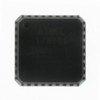
ATTINY26-16MU Atmel, ATTINY26-16MU Datasheet - Page 46

ATTINY26-16MU
Manufacturer Part Number
ATTINY26-16MU
Description
IC AVR MCU 2K 16MHZ IND 32-QFN
Manufacturer
Atmel
Series
AVR® ATtinyr
Specifications of ATTINY26-16MU
Core Processor
AVR
Core Size
8-Bit
Speed
16MHz
Connectivity
USI
Peripherals
Brown-out Detect/Reset, POR, PWM, WDT
Number Of I /o
16
Program Memory Size
2KB (1K x 16)
Program Memory Type
FLASH
Eeprom Size
128 x 8
Ram Size
128 x 8
Voltage - Supply (vcc/vdd)
4.5 V ~ 5.5 V
Data Converters
A/D 11x10b
Oscillator Type
Internal
Operating Temperature
-40°C ~ 85°C
Package / Case
32-VQFN Exposed Pad, 32-HVQFN, 32-SQFN, 32-DHVQFN
Processor Series
ATTINY2x
Core
AVR8
Data Bus Width
8 bit
Data Ram Size
128 B
Interface Type
2-Wire, ISP, SM-Bus, SPI, UART, USI
Maximum Clock Frequency
16 MHz
Number Of Programmable I/os
16
Number Of Timers
2
Operating Supply Voltage
4.5 V to 5.5 V
Maximum Operating Temperature
+ 85 C
Mounting Style
SMD/SMT
3rd Party Development Tools
EWAVR, EWAVR-BL
Development Tools By Supplier
ATAVRDRAGON, ATSTK500, ATSTK600, ATAVRISP2, ATAVRONEKIT
Minimum Operating Temperature
- 40 C
On-chip Adc
10 bit, 11 Channel
Package
32MLF EP
Device Core
AVR
Family Name
ATtiny
Maximum Speed
16 MHz
For Use With
ATSTK600-DIP40 - STK600 SOCKET/ADAPTER 40-PDIP770-1007 - ISP 4PORT ATMEL AVR MCU SPI/JTAGATAVRISP2 - PROGRAMMER AVR IN SYSTEMATSTK505 - ADAPTER KIT FOR 14PIN AVR MCU
Lead Free Status / RoHS Status
Lead free / RoHS Compliant
Available stocks
Company
Part Number
Manufacturer
Quantity
Price
Company:
Part Number:
ATTINY26-16MU
Manufacturer:
ATMEL
Quantity:
7 119
Unconnected Pins
Alternate Port
Functions
46
ATtiny26(L)
If some pins are unused, it is recommended to ensure that these pins have a defined level. Even
though most of the digital inputs are disabled in the deep sleep modes as described above, float-
ing inputs should be avoided to reduce current consumption in all other modes where the digital
inputs are enabled (Reset, Active mode, and Idle mode).
The simplest method to ensure a defined level of an unused pin, is to enable the internal pullup.
In this case, the pullup will be disabled during reset. If low power consumption during reset is
important, it is recommended to use an external pullup or pulldown. Connecting unused pins
directly to V
accidentally configured as an output.
Most port pins have alternate functions in addition to being general digital I/Os. Figure 35 shows
how the port pin control signals from the simplified Figure 32 can be overridden by alternate
functions. The overriding signals may not be present in all port pins, but the figure serves as a
generic description applicable to all port pins in the AVR microcontroller family.
Figure 35. Alternate Port Functions
Note:
1. WPx, WDx, RLx, RPx, and RDx are common to all pins within the same port. clk
PUOExn:
PUOVxn:
DDOExn:
DDOVxn:
PVOExn:
PVOVxn:
DIEOExn: Pxn DIGITAL INPUT-ENABLE OVERRIDE ENABLE
DIEOVxn: Pxn DIGITAL INPUT-ENABLE OVERRIDE VALUE
SLEEP:
Pxn
and PUD are common to all ports. All other signals are unique for each pin.
CC
or GND is not recommended, since this may cause excessive currents if the pin is
Pxn PULL-UP OVERRIDE ENABLE
Pxn PULL-UP OVERRIDE VALUE
Pxn DATA DIRECTION OVERRIDE ENABLE
Pxn DATA DIRECTION OVERRIDE VALUE
Pxn PORT VALUE OVERRIDE ENABLE
Pxn PORT VALUE OVERRIDE VALUE
SLEEP CONTROL
1
0
1
0
1
0
1
0
(1)
PUOExn
PUOVxn
DDOExn
DDOVxn
PVOExn
PVOVxn
DIEOExn
DIEOVxn
SLEEP
PUD:
WDx:
RDx:
RRx:
WPx:
RPx:
clk
DIxn:
AIOxn:
SYNCHRONIZER
D
L
I/O
SET
CLR
:
Q
Q
WRITE DDRx
WRITE PORTx
PULLUP DISABLE
READ DDRx
READ PORTx REGISTER
READ PORTx PIN
I/O CLOCK
DIGITAL INPUT PIN n ON PORTx
ANALOG INPUT/OUTPUT PIN n ON PORTx
D
PINxn
CLR
Q
Q
RESET
RESET
PORTxn
Q
Q
DDxn
Q
Q
CLR
CLR
D
D
clk
PUD
WDx
RDx
WPx
RRx
DIxn
AIOxn
RPx
I/O
1477K–AVR–08/10
I/O
, SLEEP,


