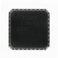
ATTINY26-16MU Atmel, ATTINY26-16MU Datasheet - Page 94

ATTINY26-16MU
Manufacturer Part Number
ATTINY26-16MU
Description
IC AVR MCU 2K 16MHZ IND 32-QFN
Manufacturer
Atmel
Series
AVR® ATtinyr
Specifications of ATTINY26-16MU
Core Processor
AVR
Core Size
8-Bit
Speed
16MHz
Connectivity
USI
Peripherals
Brown-out Detect/Reset, POR, PWM, WDT
Number Of I /o
16
Program Memory Size
2KB (1K x 16)
Program Memory Type
FLASH
Eeprom Size
128 x 8
Ram Size
128 x 8
Voltage - Supply (vcc/vdd)
4.5 V ~ 5.5 V
Data Converters
A/D 11x10b
Oscillator Type
Internal
Operating Temperature
-40°C ~ 85°C
Package / Case
32-VQFN Exposed Pad, 32-HVQFN, 32-SQFN, 32-DHVQFN
Processor Series
ATTINY2x
Core
AVR8
Data Bus Width
8 bit
Data Ram Size
128 B
Interface Type
2-Wire, ISP, SM-Bus, SPI, UART, USI
Maximum Clock Frequency
16 MHz
Number Of Programmable I/os
16
Number Of Timers
2
Operating Supply Voltage
4.5 V to 5.5 V
Maximum Operating Temperature
+ 85 C
Mounting Style
SMD/SMT
3rd Party Development Tools
EWAVR, EWAVR-BL
Development Tools By Supplier
ATAVRDRAGON, ATSTK500, ATSTK600, ATAVRISP2, ATAVRONEKIT
Minimum Operating Temperature
- 40 C
On-chip Adc
10 bit, 11 Channel
Package
32MLF EP
Device Core
AVR
Family Name
ATtiny
Maximum Speed
16 MHz
For Use With
ATSTK600-DIP40 - STK600 SOCKET/ADAPTER 40-PDIP770-1007 - ISP 4PORT ATMEL AVR MCU SPI/JTAGATAVRISP2 - PROGRAMMER AVR IN SYSTEMATSTK505 - ADAPTER KIT FOR 14PIN AVR MCU
Lead Free Status / RoHS Status
Lead free / RoHS Compliant
Available stocks
Company
Part Number
Manufacturer
Quantity
Price
Company:
Part Number:
ATTINY26-16MU
Manufacturer:
ATMEL
Quantity:
7 119
Analog to
Digital
Converter
Features
94
ATtiny26(L)
•
•
•
•
•
•
•
•
•
•
•
•
•
•
The ATtiny26(L) features a 10-bit successive approximation ADC. The ADC is connected to an
11-channel Analog Multiplexer which allows eight differential voltage input combinations or 11
single-ended voltage inputs constructed from seven pins from Port A and four pins from Port B.
Seven of the differential inputs are equipped with a programmable gain stage, providing amplifi-
cation steps of 0 dB (1x) and 26 dB (20x) on the differential input voltage before the A/D
conversion. There are four groups of three differential analog input channel selections. All input
channels in each group share a common negative terminal, while another ADC input can be
selected as the positive input terminal. The single-ended voltage inputs refer to 0V (GND).
The ADC contains a Sample and Hold Amplifier which ensures that the input voltage to the ADC
is held at a constant level during conversion. A block diagram of the ADC is shown in Figure 51.
The ADC has an analog supply voltage pin, AVCC. The voltage on AVCC must not differ more
than ±0.3V from V
how to connect these pins.
An internal reference voltage of nominally 2.56V is provided On-chip, and this reference may be
externally decoupled at the AREF pin by a capacitor.
10-bit Resolution
±2 LSB Absolute Accuracy
0.5 LSB Integral Non-linearity
Optional Offset Cancellation
13 - 260 µs Conversion Time
11 Multiplexed Single Ended Input Channels
8 Differential Input Channels
7 Differential Input Channels with Optional Gain of 20x
Optional Left Adjustment for ADC Result Readout
0 - AVCC ADC Input Voltage Range
Selectable ADC Reference Voltage
Free Running or Single Conversion Mode
Interrupt on ADC Conversion Complete
Sleep Mode Noise Canceler
CC
. See the paragraph “ADC Noise Canceling Techniques” on page 105 on
1477K–AVR–08/10


