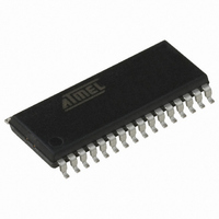
AT90PWM3B-16SU Atmel, AT90PWM3B-16SU Datasheet - Page 190

AT90PWM3B-16SU
Manufacturer Part Number
AT90PWM3B-16SU
Description
IC MCU AVR RISC 8K FLASH 32-SOIC
Manufacturer
Atmel
Series
AVR® 90PWM Lightingr
Specifications of AT90PWM3B-16SU
Core Processor
AVR
Core Size
8-Bit
Speed
16MHz
Connectivity
SPI, UART/USART
Peripherals
Brown-out Detect/Reset, POR, PWM, WDT
Number Of I /o
27
Program Memory Size
8KB (8K x 8)
Program Memory Type
FLASH
Eeprom Size
512 x 8
Ram Size
512 x 8
Voltage - Supply (vcc/vdd)
2.7 V ~ 5.5 V
Data Converters
A/D 11x10b; D/A 1x10b
Oscillator Type
Internal
Operating Temperature
-40°C ~ 105°C
Package / Case
32-SOIC (7.5mm Width)
Processor Series
AT90PWMx
Core
AVR8
Data Bus Width
8 bit
Data Ram Size
512 B
Interface Type
SPI/USART
Maximum Clock Frequency
16 MHz
Number Of Programmable I/os
27
Number Of Timers
2
Operating Supply Voltage
2.7 V to 5.5 V
Maximum Operating Temperature
+ 105 C
Mounting Style
SMD/SMT
3rd Party Development Tools
EWAVR, EWAVR-BL
Development Tools By Supplier
ATAVRDRAGON, ATSTK500, ATSTK600, ATAVRISP2, ATAVRONEKIT, ATAVRFBKIT, ATAVRISP2
Minimum Operating Temperature
- 40 C
On-chip Adc
11-ch x 10-bit
On-chip Dac
1-chx10-bit
Controller Family/series
AVR PWM
Eeprom Memory Size
512Byte
Ram Memory Size
512Byte
Cpu Speed
16MHz
Rohs Compliant
Yes
For Use With
ATSTK600-SOIC - STK600 SOCKET/ADAPTER FOR SOIC770-1007 - ISP 4PORT ATMEL AVR MCU SPI/JTAGATAVRMC200 - KIT EVAL FOR AT90PWM3 ASYNCATAVRFBKIT - KIT DEMO BALLAST FOR AT90PWM2ATAVRISP2 - PROGRAMMER AVR IN SYSTEMATSTK520 - ADAPTER KIT FOR 90PWM
Lead Free Status / RoHS Status
Lead free / RoHS Compliant
Available stocks
Company
Part Number
Manufacturer
Quantity
Price
Company:
Part Number:
AT90PWM3B-16SU
Manufacturer:
Atmel
Quantity:
4 000
Part Number:
AT90PWM3B-16SU
Manufacturer:
MICROCHIP/微芯
Quantity:
20 000
- Current page: 190 of 361
- Download datasheet (7Mb)
18.6.1
18.6.2
190
AT90PWM2/3/2B/3B
Sending Frames with 5 to 8 Data Bit
Sending Frames with 9 Data Bit
chronous operation is used, the clock on the XCK pin will be overridden and used as
transmission clock.
A data transmission is initiated by loading the transmit buffer with the data to be transmitted. The
CPU can load the transmit buffer by writing to the UDR I/O location. The buffered data in the
transmit buffer will be moved to the Shift Register when the Shift Register is ready to send a new
frame. The Shift Register is loaded with new data if it is in idle state (no ongoing transmission) or
immediately after the last stop bit of the previous frame is transmitted. When the Shift Register is
loaded with new data, it will transfer one complete frame at the rate given by the Baud Register,
U2X bit or by XCK depending on mode of operation.
The following code examples show a simple USART transmit function based on polling of the
Data Register Empty (UDRE) flag. When using frames with less than eight bits, the most signifi-
cant bits written to the UDR are ignored. The USART has to be initialized before the function can
be used. For the assembly code, the data to be sent is assumed to be stored in Register R16
Note:
The function simply waits for the transmit buffer to be empty by checking the UDRE flag, before
loading it with new data to be transmitted. If the Data Register Empty interrupt is utilized, the
interrupt routine writes the data into the buffer.
If 9-bit characters are used (UCSZ = 7), the ninth bit must be written to the TXB8 bit in UCSRB
before the low byte of the character is written to UDR. The following code examples show a
transmit function that handles 9-bit characters. For the assembly code, the data to be sent is
assumed to be stored in registers R17:R16.
Assembly Code Example
C Code Example
TABLE 3.
USART_Transmit:
void USART_Transmit( unsigned char data )
{
}
; Wait for empty transmit buffer
sbis UCSRA,UDRE
rjmp USART_Transmit
; Put data (r16) into buffer, sends the data
sts UDR,r16
ret
/* Wait for empty transmit buffer */
while ( !( UCSRA & (1<<UDRE)) )
/* Put data into buffer, sends the data */
UDR = data;
1. The example code assumes that the part specific header file is included.
For I/O Registers located in extended I/O map, “IN”, “OUT”, “SBIS”, “SBIC”, “CBI”, and “SBI”
instructions must be replaced with instructions that allow access to extended I/O. Typically
“LDS” and “STS” combined with “SBRS”, “SBRC”, “SBR”, and “CBR”.
;
(1)
(1)
4317J–AVR–08/10
.
Related parts for AT90PWM3B-16SU
Image
Part Number
Description
Manufacturer
Datasheet
Request
R

Part Number:
Description:
Manufacturer:
Atmel Corporation
Datasheet:

Part Number:
Description:
IC MCU AVR RISC 8K FLASH 32-QFN
Manufacturer:
Atmel
Datasheet:

Part Number:
Description:
MCU AVR 8K FLASH 16MHA 32SOIC
Manufacturer:
Atmel
Datasheet:

Part Number:
Description:
IC AVR MCU FLASH 8K 32QFN
Manufacturer:
Atmel
Datasheet:

Part Number:
Description:
IC AVR MCU FLASH 8K 32SOIC
Manufacturer:
Atmel
Datasheet:

Part Number:
Description:
MCU AVR 8K FLASH 16MHZ 32-QFN
Manufacturer:
Atmel
Datasheet:

Part Number:
Description:
DEV KIT FOR AVR/AVR32
Manufacturer:
Atmel
Datasheet:

Part Number:
Description:
INTERVAL AND WIPE/WASH WIPER CONTROL IC WITH DELAY
Manufacturer:
ATMEL Corporation
Datasheet:

Part Number:
Description:
Low-Voltage Voice-Switched IC for Hands-Free Operation
Manufacturer:
ATMEL Corporation
Datasheet:

Part Number:
Description:
MONOLITHIC INTEGRATED FEATUREPHONE CIRCUIT
Manufacturer:
ATMEL Corporation
Datasheet:

Part Number:
Description:
AM-FM Receiver IC U4255BM-M
Manufacturer:
ATMEL Corporation
Datasheet:

Part Number:
Description:
Monolithic Integrated Feature Phone Circuit
Manufacturer:
ATMEL Corporation
Datasheet:

Part Number:
Description:
Multistandard Video-IF and Quasi Parallel Sound Processing
Manufacturer:
ATMEL Corporation
Datasheet:


