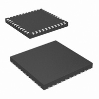
PIC18F47J13-I/ML Microchip Technology, PIC18F47J13-I/ML Datasheet - Page 297

PIC18F47J13-I/ML
Manufacturer Part Number
PIC18F47J13-I/ML
Description
IC PIC MCU 128KB FLASH 44QFN
Manufacturer
Microchip Technology
Series
PIC® XLP™ 18Fr
Datasheets
1.PIC18LF24J10-ISS.pdf
(32 pages)
2.PIC18F26J13-ISS.pdf
(496 pages)
3.PIC18F26J13-ISS.pdf
(558 pages)
4.PIC18F26J13-ISS.pdf
(12 pages)
Specifications of PIC18F47J13-I/ML
Core Size
8-Bit
Program Memory Size
128KB (64K x 16)
Core Processor
PIC
Speed
48MHz
Connectivity
I²C, LIN, SPI, UART/USART
Peripherals
Brown-out Detect/Reset, POR, PWM, WDT
Number Of I /o
34
Program Memory Type
FLASH
Ram Size
3.8K x 8
Voltage - Supply (vcc/vdd)
2.15 V ~ 3.6 V
Data Converters
A/D 13x10b/12b
Oscillator Type
Internal
Operating Temperature
-40°C ~ 85°C
Package / Case
*
Controller Family/series
PIC18
Cpu Speed
48MHz
Digital Ic Case Style
QFN
Supply Voltage Range
1.8V To 5.5V
Embedded Interface Type
I2C, SPI, USART
Rohs Compliant
Yes
Processor Series
PIC18F
Core
PIC
Data Bus Width
8 bit
Data Ram Size
4 KB
Interface Type
I2C, SPI, EUSART
Maximum Clock Frequency
48 MHz
Number Of Programmable I/os
25
Number Of Timers
8
Operating Supply Voltage
2 V to 3.6 V
Maximum Operating Temperature
+ 85 C
Mounting Style
SMD/SMT
3rd Party Development Tools
52715-96, 52716-328, 52717-734, 52712-325, EWPIC18
Development Tools By Supplier
DM164128, DM180021, DM183026-2, DV164131, MA180030, DM183022, DM183032, DV164136, MA180024
Minimum Operating Temperature
- 40 C
On-chip Adc
12 bit, 13 Channel
Lead Free Status / RoHS Status
Lead free / RoHS Compliant
For Use With
MA180030 - BOARD DEMO PIC18F47J13 FS USBMA180029 - BOARD DEMO PIC18F47J53 FS USB
Eeprom Size
-
Lead Free Status / Rohs Status
Details
- PIC18LF24J10-ISS PDF datasheet
- PIC18F26J13-ISS PDF datasheet #2
- PIC18F26J13-ISS PDF datasheet #3
- PIC18F26J13-ISS PDF datasheet #4
- Current page: 297 of 558
- Download datasheet (5Mb)
20.3.6
The master can initiate the data transfer at any time
because it controls the SCKx. The master determines
when the slave (Processor 2, Figure 20-2) is to
broadcast data by the software protocol.
In Master mode, the data is transmitted/received as
soon as the SSPxBUF register is written to. If the SPI
is only going to receive, the SDOx output could be dis-
abled (programmed as an input). The SSPxSR register
will continue to shift in the signal present on the SDIx
pin at the programmed clock rate. As each byte is
received, it will be loaded into the SSPxBUF register as
if it is a normal received byte (interrupts and status bits
are appropriately set). This could be useful in receiver
applications as a “Line Activity Monitor” mode.
The CKP is selected by appropriately programming the
CKP bit (SSPxCON1<4>). This then, would give
waveforms for SPI communication, as illustrated in
FIGURE 20-3:
2010 Microchip Technology Inc.
Note:
Write to
SSPxBUF
SCKx
(CKP = 0
CKE = 0)
SCKx
(CKP = 1
CKE = 0)
SCKx
(CKP = 0
CKE = 1)
SCKx
(CKP = 1
CKE = 1)
SDOx
(CKE = 0)
SDOx
(CKE = 1)
SDIx
(SMP = 0)
Input
Sample
(SMP = 0)
SDIx
(SMP = 1)
Input
Sample
(SMP = 1)
SSPxIF
SSPxSR to
SSPxBUF
To avoid lost data in Master mode, a read of
the SSPxBUF must be performed to clear the
Buffer Full (BF) detect bit (SSPxSTAT<0>)
between each transmission.
MASTER MODE
SPI MODE WAVEFORM (MASTER MODE)
bit 7
bit 7
bit 7
bit 7
bit 6
bit 6
bit 5
bit 5
Preliminary
bit 4
bit 4
PIC18F47J13 FAMILY
bit 3
bit 3
Figure 20-3, Figure 20-5 and Figure 20-6, where the
Most Significant Byte (MSB) is transmitted first. In
Master mode, the SPI clock rate (bit rate) is
user-programmable to be one of the following:
• F
• F
• F
• F
• Timer2 output/2
When using the Timer2 output/2 option, the Period
Register 2 (PR2) can be used to determine the SPI bit
rate. However, only PR2 values of 0x01 to 0xFF are
valid in this mode.
Figure 20-3 illustrates the waveforms for Master mode.
When the CKE bit is set, the SDOx data is valid before
there is a clock edge on SCKx. The change of the input
sample is shown based on the state of the SMP bit. The
time when the SSPxBUF is loaded with the received
data is shown.
OSC
OSC
OSC
OSC
/4 (or T
/8 (or 2 • T
/16 (or 4 • T
/64 (or 16 • T
bit 2
bit 2
CY
)
bit 1
bit 1
CY
CY
)
CY
)
)
bit 0
bit 0
bit 0
bit 0
DS39974A-page 297
Next Q4 Cycle
after Q2
4 Clock
Modes
Related parts for PIC18F47J13-I/ML
Image
Part Number
Description
Manufacturer
Datasheet
Request
R

Part Number:
Description:
Manufacturer:
Microchip Technology Inc.
Datasheet:

Part Number:
Description:
Manufacturer:
Microchip Technology Inc.
Datasheet:

Part Number:
Description:
Manufacturer:
Microchip Technology Inc.
Datasheet:

Part Number:
Description:
Manufacturer:
Microchip Technology Inc.
Datasheet:

Part Number:
Description:
Manufacturer:
Microchip Technology Inc.
Datasheet:

Part Number:
Description:
Manufacturer:
Microchip Technology Inc.
Datasheet:

Part Number:
Description:
Manufacturer:
Microchip Technology Inc.
Datasheet:

Part Number:
Description:
Manufacturer:
Microchip Technology Inc.
Datasheet:


