PIC18F47J13-I/ML Microchip Technology, PIC18F47J13-I/ML Datasheet - Page 367
PIC18F47J13-I/ML
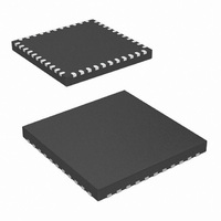
Manufacturer Part Number
PIC18F47J13-I/ML
Description
IC PIC MCU 128KB FLASH 44QFN
Manufacturer
Microchip Technology
Series
PIC® XLP™ 18Fr
Datasheets
1.PIC18LF24J10-ISS.pdf
(32 pages)
2.PIC18F26J13-ISS.pdf
(496 pages)
3.PIC18F26J13-ISS.pdf
(558 pages)
4.PIC18F26J13-ISS.pdf
(12 pages)
Specifications of PIC18F47J13-I/ML
Core Size
8-Bit
Program Memory Size
128KB (64K x 16)
Core Processor
PIC
Speed
48MHz
Connectivity
I²C, LIN, SPI, UART/USART
Peripherals
Brown-out Detect/Reset, POR, PWM, WDT
Number Of I /o
34
Program Memory Type
FLASH
Ram Size
3.8K x 8
Voltage - Supply (vcc/vdd)
2.15 V ~ 3.6 V
Data Converters
A/D 13x10b/12b
Oscillator Type
Internal
Operating Temperature
-40°C ~ 85°C
Package / Case
*
Controller Family/series
PIC18
Cpu Speed
48MHz
Digital Ic Case Style
QFN
Supply Voltage Range
1.8V To 5.5V
Embedded Interface Type
I2C, SPI, USART
Rohs Compliant
Yes
Processor Series
PIC18F
Core
PIC
Data Bus Width
8 bit
Data Ram Size
4 KB
Interface Type
I2C, SPI, EUSART
Maximum Clock Frequency
48 MHz
Number Of Programmable I/os
25
Number Of Timers
8
Operating Supply Voltage
2 V to 3.6 V
Maximum Operating Temperature
+ 85 C
Mounting Style
SMD/SMT
3rd Party Development Tools
52715-96, 52716-328, 52717-734, 52712-325, EWPIC18
Development Tools By Supplier
DM164128, DM180021, DM183026-2, DV164131, MA180030, DM183022, DM183032, DV164136, MA180024
Minimum Operating Temperature
- 40 C
On-chip Adc
12 bit, 13 Channel
Lead Free Status / RoHS Status
Lead free / RoHS Compliant
For Use With
MA180030 - BOARD DEMO PIC18F47J13 FS USBMA180029 - BOARD DEMO PIC18F47J53 FS USB
Eeprom Size
-
Lead Free Status / Rohs Status
Details


22.0
The Analog-to-Digital (A/D) Converter module in the
PIC18F47J13 family of devices has 10 inputs for the
28-pin devices and 13 inputs for the 44-pin devices.
This module allows conversion of an analog input
signal to a corresponding 10 or 12-bit digital number.
The module has these registers:
• A/D Control Register 0 (ADCON0)
• A/D Control Register 1 (ADCON1)
• A/D Port Configuration Register 0 (ANCON0)
• A/D Port Configuration Register 1 (ANCON1)
• A/D Result Registers (ADRESH and ADRESL)
• A/D Trigger Register (ADCTRIG)
• Configuration Register 3 High (ADCSEL,
2010 Microchip Technology Inc.
CONFIG3H<1>)
10/12-BIT ANALOG-TO-DIGITAL
CONVERTER (A/D) MODULE
Preliminary
PIC18F47J13 FAMILY
The ADCON0 register, shown in Register 22-1,
controls the operation of the A/D module.
The ADCON1 register, shown in Register 22-2, config-
ures the A/D clock source, programmed acquisition
time and justification. The ANCON0 and ANCON1
registers, in Register 22-1 and Register 22-2, configure
the functions of the port pins.
The ADCSEL Configuration bit (CONFIG3H<1>) sets
the module for 10 or 12-bit conversions. The 10-Bit
Conversion mode is useful for applications that favor
conversion speed over conversion resolution.
DS39974A-page 367
Related parts for PIC18F47J13-I/ML
Image
Part Number
Description
Manufacturer
Datasheet
Request
R

Part Number:
Description:
Manufacturer:
Microchip Technology Inc.
Datasheet:
Part Number:
Description:
Manufacturer:
Microchip Technology Inc.
Datasheet:
Part Number:
Description:
Manufacturer:
Microchip Technology Inc.
Datasheet:
Part Number:
Description:
Manufacturer:
Microchip Technology Inc.
Datasheet:
Part Number:
Description:
Manufacturer:
Microchip Technology Inc.
Datasheet:
Part Number:
Description:
Manufacturer:
Microchip Technology Inc.
Datasheet:
Part Number:
Description:
Manufacturer:
Microchip Technology Inc.
Datasheet:
Part Number:
Description:
Manufacturer:
Microchip Technology Inc.
Datasheet: