PIC24FJ128GA010-I/PT Microchip Technology, PIC24FJ128GA010-I/PT Datasheet - Page 94
PIC24FJ128GA010-I/PT
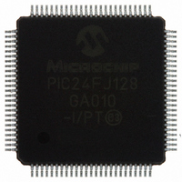
Manufacturer Part Number
PIC24FJ128GA010-I/PT
Description
IC PIC MCU FLASH 128K 100TQFP
Manufacturer
Microchip Technology
Series
PIC® 24Fr
Datasheets
1.PIC24FJ16GA002-ISS.pdf
(52 pages)
2.PIC24FJ64GA006-IPT.pdf
(240 pages)
3.PIC24FJ64GA006-IPT.pdf
(22 pages)
4.PIC24FJ128GA008-IPT.pdf
(12 pages)
5.PIC24FJ128GA006-IPT.pdf
(231 pages)
6.PIC24FJ128GA010-IPT.pdf
(230 pages)
Specifications of PIC24FJ128GA010-I/PT
Core Size
16-Bit
Program Memory Size
128KB (43K x 24)
Core Processor
PIC
Speed
16MHz
Connectivity
I²C, PMP, SPI, UART/USART
Peripherals
Brown-out Detect/Reset, POR, PWM, WDT
Number Of I /o
84
Program Memory Type
FLASH
Ram Size
8K x 8
Voltage - Supply (vcc/vdd)
2 V ~ 3.6 V
Data Converters
A/D 16x10b
Oscillator Type
Internal
Operating Temperature
-40°C ~ 85°C
Package / Case
100-TFQFP
Controller Family/series
PIC24
No. Of I/o's
84
Ram Memory Size
8KB
Cpu Speed
32MHz
No. Of Timers
5
No. Of Pwm Channels
5
Embedded Interface Type
EUART, I2C, PSP, SPI
Rohs Compliant
Yes
Processor Series
PIC24FJ
Core
PIC
Data Bus Width
16 bit
Data Ram Size
8 KB
Interface Type
SPI, I2C, USART
Maximum Clock Frequency
16 MHz
Number Of Programmable I/os
54
Number Of Timers
5
Maximum Operating Temperature
+ 85 C
Mounting Style
SMD/SMT
3rd Party Development Tools
52713-733, 52714-737, 53276-922, EWDSPIC
Development Tools By Supplier
PG164130, DV164035, DV244005, DV164005, PG164120, DM240001, DM240011
Minimum Operating Temperature
- 40 C
On-chip Adc
10 bit, 16 Channel
Package
100TQFP
Device Core
PIC
Family Name
PIC24
Maximum Speed
16 MHz
Operating Supply Voltage
2.5|3.3 V
Lead Free Status / RoHS Status
Lead free / RoHS Compliant
For Use With
DM240011 - KIT STARTER MPLAB FOR PIC24F MCUAC164333 - MODULE SKT FOR PM3 100QFPDV164033 - KIT START EXPLORER 16 MPLAB ICD2MA160011 - DAUGHTER BOARD PICDEM LCD 16F91XDM240001 - BOARD DEMO PIC24/DSPIC33/PIC32
Eeprom Size
-
Lead Free Status / Rohs Status
Details
Available stocks
Company
Part Number
Manufacturer
Quantity
Price
Company:

Part Number:
PIC24FJ128GA010-I/PT
Manufacturer:
Microchi
Quantity:
627
Company:
Part Number:
PIC24FJ128GA010-I/PT
Manufacturer:
MICROCHIP
Quantity:
212
Company:
Part Number:
PIC24FJ128GA010-I/PT
Manufacturer:
Microchip Technology
Quantity:
10 000


PIC24FJ128GA FAMILY
7.2
The oscillator source (and operating mode) that is
used at a device Power-on Reset event is selected
using Configuration bit settings. The oscillator Config-
uration bit settings are located in the Configuration
registers
Section 23.1
details.) The Primary Oscillator Configuration bits,
POSCMD1:POSCMD0 (Configuration Word 2<1:0>),
and the Initial Oscillator Select Configuration bits,
FNOSC2:FNOSC0
select the oscillator source that is used at a Power-on
Reset. The FRC primary oscillator with postscaler
(FRCDIV) is the default (unprogrammed) selection.
TABLE 7-1:
7.3
The operation of the oscillator is controlled by three
Special Function Registers:
• OSCCON
• CLKDIV
• OSCTUN
The OSCCON register (Register 7-1) is the main con-
trol register for the oscillator. It controls clock source
switching, and allows the monitoring of clock sources.
DS39747C-page 92
Fast RC Oscillator with Postscaler
(FRCDIV)
(Reserved)
Low-Power RC Oscillator (LPRC)
Secondary (Timer1) Oscillator
(SOSC)
Primary Oscillator (HS) with PLL
Module (HSPLL)
Primary Oscillator (XT) with PLL
Module (ECPLL)
Primary Oscillator (EC) with PLL
Module (XTPLL)
Primary Oscillator (HS)
Primary Oscillator (XT)
Primary Oscillator (EC)
Fast RC Oscillator with PLL Module
(FRCPLL)
Fast RC Oscillator (FRC)
Note 1:
2:
Oscillator Configuration
Control Registers
Oscillator Mode
in
OSC2 pin function is determined by the OSCIOFNC Configuration bit.
This is the default oscillator mode for an unprogrammed (erased) device.
the
“Configuration
CONFIGURATION BIT VALUES FOR CLOCK SELECTION
program
(Configuration Word 2<10:8>),
memory
Bits”
Oscillator Source
for
(refer
Secondary
Internal
Internal
Internal
Primary
Primary
Primary
Primary
Primary
Primary
Internal
Internal
further
Preliminary
to
The secondary oscillator, or one of the internal
oscillators, may be chosen by programming these bit
locations.
The Configuration bits allow users to choose between
the various clock modes, shown in Table 7-1.
7.2.1
The FCKSM Configuration bits (Configuration Word 2<7:6>)
are used to jointly configure device clock switching and
the Fail-Safe Clock Monitor (FSCM). Clock switching is
enabled only when FCKSM1 is programmed (‘0’). The
FSCM is enabled only when FCKSM1:FCKSM0 are
both programmed (‘00’).
The Clock Divider register (Register 7-2) controls the
features associated with Doze mode, as well as the
postscaler for the FRC oscillator.
The FRC Oscillator Tune register (Register 7-3) allows
the user to fine tune the FRC oscillator over a range of
approximately ±12%. Each bit increment or decrement
changes the factory calibrated frequency of the FRC
oscillator by a fixed amount.
POSCMD1:
POSCMD0
00
00
00
00
10
01
00
10
01
00
00
00
CLOCK SWITCHING MODE
CONFIGURATION BITS
© 2006 Microchip Technology Inc.
FNOSC2:
FNOSC0
111
110
101
100
011
011
011
010
010
010
001
000
Note
1, 2
1
1
1
1
1
Related parts for PIC24FJ128GA010-I/PT
Image
Part Number
Description
Manufacturer
Datasheet
Request
R

Part Number:
Description:
General Purpose, 16-Bit Flash Microcontrollers
Manufacturer:
MICROCHIP [Microchip Technology]
Datasheet:

Part Number:
Description:
Manufacturer:
Microchip Technology Inc.
Datasheet:
Part Number:
Description:
Manufacturer:
Microchip Technology Inc.
Datasheet:
Part Number:
Description:
Manufacturer:
Microchip Technology Inc.
Datasheet:
Part Number:
Description:
Manufacturer:
Microchip Technology Inc.
Datasheet:
Part Number:
Description:
Manufacturer:
Microchip Technology Inc.
Datasheet:
Part Number:
Description:
Manufacturer:
Microchip Technology Inc.
Datasheet:
Part Number:
Description:
Manufacturer:
Microchip Technology Inc.
Datasheet:
Part Number:
Description:
Manufacturer:
Microchip Technology Inc.
Datasheet: