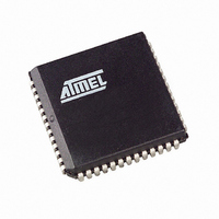
AT89C5131A-S3SUM Atmel, AT89C5131A-S3SUM Datasheet - Page 33

AT89C5131A-S3SUM
Manufacturer Part Number
AT89C5131A-S3SUM
Description
IC 8051 MCU FLASH 32K USB 52PLCC
Manufacturer
Atmel
Series
AT89C513xr
Datasheet
1.AT89C5130A-PUTUM.pdf
(188 pages)
Specifications of AT89C5131A-S3SUM
Core Processor
C52X2
Core Size
8-Bit
Speed
48MHz
Connectivity
I²C, SPI, UART/USART, USB
Peripherals
LED, POR, PWM, WDT
Number Of I /o
34
Program Memory Size
32KB (32K x 8)
Program Memory Type
FLASH
Eeprom Size
4K x 8
Ram Size
1.25K x 8
Voltage - Supply (vcc/vdd)
2.7 V ~ 5.5 V
Oscillator Type
Internal
Operating Temperature
-40°C ~ 85°C
Package / Case
52-PLCC
Processor Series
AT89x
Core
8051
Data Bus Width
8 bit
Data Ram Size
1.25 KB
Interface Type
2-Wire, EUART, SPI, USB
Maximum Clock Frequency
48 MHz
Number Of Programmable I/os
34
Number Of Timers
16 bit
Operating Supply Voltage
2.7 V to 5.5 V
Maximum Operating Temperature
+ 85 C
Mounting Style
SMD/SMT
3rd Party Development Tools
PK51, CA51, A51, ULINK2
Development Tools By Supplier
AT89STK-05
Minimum Operating Temperature
- 40 C
Package
52PLCC
Device Core
8051
Family Name
89C
Maximum Speed
48 MHz
For Use With
AT89OCD-01 - USB EMULATOR FOR AT8XC51 MCUAT89STK-10 - KIT EVAL APPL MASS STORAGEAT89STK-05 - KIT STARTER FOR AT89C5131
Lead Free Status / RoHS Status
Lead free / RoHS Compliant
Data Converters
-
Lead Free Status / Rohs Status
Details
Available stocks
Company
Part Number
Manufacturer
Quantity
Price
Company:
Part Number:
AT89C5131A-S3SUM
Manufacturer:
ATMEL
Quantity:
46
8.3.3
8.3.4
8.3.5
4337K–USB–04/08
Status of the Flash Memory
Selecting FM0/FM1
Loading the Column Latches
Table 8-3.
The Flash memory enters a busy state as soon as programming is launched. In this state, the
memory is not available for fetching code. Thus to avoid any erratic execution during program-
ming, the CPU enters Idle mode. Exit is automatically performed at the end of programming.
Note:
The bit FBUSY in FCON register is used to indicate the status of programming.
FBUSY is set when programming is in progress.
The bit ENBOOT in AUXR1 register is used to choose between FM0 and FM1 mapped up to
F800h.
Any number of data from 1 byte to 128 bytes can be loaded in the column latches. This provides
the capability to program the whole memory by byte, by page or by any number of bytes in a
page.
When programming is launched, an automatic erase of the locations loaded in the column
latches is first performed, then programming is effectively done. Thus, no page or block erase is
needed and only the loaded data are programmed in the corresponding page.
The following procedure is used to load the column latches and is summarized in Figure 8-5:
• Map the column latch space by setting FPS bit.
• Load the DPTR with the address to load.
• Load Accumulator register with the data to load.
• Execute the MOVX @DPTR, A instruction.
• If needed loop the three last instructions until the page is completely loaded.
Interrupts that may occur during programming time must be disabled to avoid any spurious exit of
the idle mode.
Extra Row
Reserved
Security
Space
User
Programming Spaces
FPL3:0
A
A
A
A
5
5
5
5
FPS
X
X
X
X
X
X
X
X
Write to FCON
FMOD1
0
0
0
0
1
1
1
1
FMOD0
AT89C5130A/31A-M
0
0
1
1
0
0
1
1
Operation
No action
Write the column latches in user
space
No action
Write the column latches in extra row
space
No action
Write the fuse bits space
No action
No action
33


