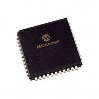
PIC16F877-20/L Microchip Technology, PIC16F877-20/L Datasheet - Page 46

PIC16F877-20/L
Manufacturer Part Number
PIC16F877-20/L
Description
IC MCU FLASH 8KX14 EE 44PLCC
Manufacturer
Microchip Technology
Series
PIC® 16Fr
Datasheets
1.PIC16F616T-ISL.pdf
(8 pages)
2.PIC16F688T-ISL.pdf
(688 pages)
3.PIC16C770-ISO.pdf
(8 pages)
4.PIC16F873-04SO.pdf
(218 pages)
5.PIC16F873-04SO.pdf
(5 pages)
6.PIC16F873-04SO.pdf
(5 pages)
Specifications of PIC16F877-20/L
Program Memory Type
FLASH
Program Memory Size
14KB (8K x 14)
Package / Case
44-PLCC
Core Processor
PIC
Core Size
8-Bit
Speed
20MHz
Connectivity
I²C, SPI, UART/USART
Peripherals
Brown-out Detect/Reset, POR, PWM, WDT
Number Of I /o
33
Eeprom Size
256 x 8
Ram Size
368 x 8
Voltage - Supply (vcc/vdd)
4 V ~ 5.5 V
Data Converters
A/D 8x10b
Oscillator Type
External
Operating Temperature
0°C ~ 70°C
Processor Series
PIC16F
Core
PIC
Data Bus Width
8 bit
Data Ram Size
368 B
Interface Type
MSSP/PSP/USART
Maximum Clock Frequency
20 MHz
Number Of Programmable I/os
33
Number Of Timers
3
Operating Supply Voltage
2 V to 5.5 V
Maximum Operating Temperature
+ 70 C
Mounting Style
SMD/SMT
3rd Party Development Tools
52715-96, 52716-328, 52717-734
Development Tools By Supplier
PG164130, DV164035, DV244005, DV164005, PG164120, ICE2000, DM163022, DV164120
Minimum Operating Temperature
0 C
On-chip Adc
8-ch x 10-bit
Data Rom Size
256 B
Height
3.87 mm
Length
16.59 mm
Supply Voltage (max)
5.5 V
Supply Voltage (min)
4 V
Width
16.59 mm
Lead Free Status / RoHS Status
Lead free / RoHS Compliant
For Use With
AC164309 - MODULE SKT FOR PM3 44PLCC444-1001 - DEMO BOARD FOR PICMICRO MCUDVA16XL441 - ADAPTER DEVICE ICE 44PLCC309-1040 - ADAPTER 44-PLCC ZIF TO 40-DIP309-1039 - ADAPTER 44-PLCC TO 40-DIPDV007003 - PROGRAMMER UNIVERSAL PROMATE II
Lead Free Status / Rohs Status
Lead free / RoHS Compliant
Available stocks
Company
Part Number
Manufacturer
Quantity
Price
Company:
Part Number:
PIC16F877-20/L
Manufacturer:
MICROCHI
Quantity:
27
Company:
Part Number:
PIC16F877-20/L
Manufacturer:
Microchip Technology
Quantity:
10 000
Part Number:
PIC16F877-20/L
Manufacturer:
MICROCHIP/微芯
Quantity:
20 000
PIC16F87X
4.4
Reading FLASH program memory is much like that of
EEPROM data memory, only two NOP instructions must
be inserted after the RD bit is set. These two instruction
cycles that the NOP instructions execute, will be used
by the microcontroller to read the data out of program
memory
EEDATH:EEDATA registers. Data will be available fol-
lowing the second NOP instruction. EEDATH and
EEDATA will hold their value until another read opera-
tion is initiated, or until they are written by firmware.
The steps to reading the FLASH program memory are:
1.
2.
3.
4.
5.
EXAMPLE 4-3:
DS30292C-page 44
BSF
BCF
MOVF
MOVWF
MOVF
MOVWF
BSF
BSF
BSF
NOP
NOP
BCF
MOVF
MOVWF
MOVF
MOVWF
Write the address to EEADRH:EEADR. Make
sure that the address is not larger than the mem-
ory size of the PIC16F87X device.
Set the EEPGD bit to point to FLASH program
memory.
Set the RD bit to start the read operation.
Execute two NOP instructions to allow the micro-
controller to read out of program memory.
Read the data from the EEDATH:EEDATA
registers.
Reading the FLASH Program
Memory
STATUS, RP1
STATUS, RP0
ADDRL, W
EEADR
ADDRH,W
EEADRH
STATUS, RP0
EECON1, EEPGD ;Point to Program memory
EECON1, RD
STATUS, RP0
EEDATA, W
DATAL
EEDATH,W
DATAH
and
insert
FLASH PROGRAM READ
;
;Bank 2
;Write the
;address bytes
;for the desired
;address to read
;Bank 3
;Start read operation
;Required two NOPs
;
;Bank 2
;DATAL = EEDATA
;
;DATAH = EEDATH
;
the
value
into
the
4.5
Writing to FLASH program memory is unique, in that
the microcontroller does not execute instructions while
programming is taking place. The oscillator continues
to run and all peripherals continue to operate and
queue interrupts, if enabled. Once the write operation
completes (specification D133), the processor begins
executing code from where it left off. The other impor-
tant difference when writing to FLASH program mem-
ory, is that the WRT configuration bit, when clear,
prevents any writes to program memory (see Table 4-1).
Just like EEPROM data memory, there are many steps
in writing to the FLASH program memory. Both address
and data values must be written to the SFRs. The
EEPGD bit must be set, and the WREN bit must be set
to enable writes. The WREN bit should be kept clear at
all times, except when writing to the FLASH Program
memory. The WR bit can only be set if the WREN bit
was set in a previous operation, i.e., they both cannot
be set in the same operation. The WREN bit should
then be cleared by firmware after the write. Clearing the
WREN bit before the write actually completes will not
terminate the write in progress.
Writes to program memory must also be prefaced with
a special sequence of instructions that prevent inad-
vertent write operations. This is a sequence of five
instructions that must be executed without interruption
for each byte written. These instructions must then be
followed by two NOP instructions to allow the microcon-
troller to setup for the write operation. Once the write is
complete, the execution of instructions starts with the
instruction after the second NOP.
The steps to write to program memory are:
1.
2.
3.
4.
5.
6.
7.
8.
9.
Write the address to EEADRH:EEADR. Make
sure that the address is not larger than the mem-
ory size of the PIC16F87X device.
Write the 14-bit data value to be programmed in
the EEDATH:EEDATA registers.
Set the EEPGD bit to point to FLASH program
memory.
Set the WREN bit to enable program operations.
Disable interrupts (if enabled).
Execute the special five instruction sequence:
• Write 55h to EECON2 in two steps (first to W,
• Write AAh to EECON2 in two steps (first to W,
• Set the WR bit
Execute two NOP instructions to allow the micro-
controller to setup for write operation.
Enable interrupts (if using interrupts).
Clear the WREN bit to disable program
operations.
then to EECON2)
then to EECON2)
Writing to the FLASH Program
Memory
2001 Microchip Technology Inc.


