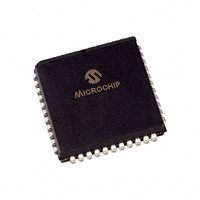
PIC16F877-20/L Microchip Technology, PIC16F877-20/L Datasheet - Page 53

PIC16F877-20/L
Manufacturer Part Number
PIC16F877-20/L
Description
IC MCU FLASH 8KX14 EE 44PLCC
Manufacturer
Microchip Technology
Series
PIC® 16Fr
Datasheets
1.PIC16F616T-ISL.pdf
(8 pages)
2.PIC16F688T-ISL.pdf
(688 pages)
3.PIC16C770-ISO.pdf
(8 pages)
4.PIC16F873-04SO.pdf
(218 pages)
5.PIC16F873-04SO.pdf
(5 pages)
6.PIC16F873-04SO.pdf
(5 pages)
Specifications of PIC16F877-20/L
Program Memory Type
FLASH
Program Memory Size
14KB (8K x 14)
Package / Case
44-PLCC
Core Processor
PIC
Core Size
8-Bit
Speed
20MHz
Connectivity
I²C, SPI, UART/USART
Peripherals
Brown-out Detect/Reset, POR, PWM, WDT
Number Of I /o
33
Eeprom Size
256 x 8
Ram Size
368 x 8
Voltage - Supply (vcc/vdd)
4 V ~ 5.5 V
Data Converters
A/D 8x10b
Oscillator Type
External
Operating Temperature
0°C ~ 70°C
Processor Series
PIC16F
Core
PIC
Data Bus Width
8 bit
Data Ram Size
368 B
Interface Type
MSSP/PSP/USART
Maximum Clock Frequency
20 MHz
Number Of Programmable I/os
33
Number Of Timers
3
Operating Supply Voltage
2 V to 5.5 V
Maximum Operating Temperature
+ 70 C
Mounting Style
SMD/SMT
3rd Party Development Tools
52715-96, 52716-328, 52717-734
Development Tools By Supplier
PG164130, DV164035, DV244005, DV164005, PG164120, ICE2000, DM163022, DV164120
Minimum Operating Temperature
0 C
On-chip Adc
8-ch x 10-bit
Data Rom Size
256 B
Height
3.87 mm
Length
16.59 mm
Supply Voltage (max)
5.5 V
Supply Voltage (min)
4 V
Width
16.59 mm
Lead Free Status / RoHS Status
Lead free / RoHS Compliant
For Use With
AC164309 - MODULE SKT FOR PM3 44PLCC444-1001 - DEMO BOARD FOR PICMICRO MCUDVA16XL441 - ADAPTER DEVICE ICE 44PLCC309-1040 - ADAPTER 44-PLCC ZIF TO 40-DIP309-1039 - ADAPTER 44-PLCC TO 40-DIPDV007003 - PROGRAMMER UNIVERSAL PROMATE II
Lead Free Status / Rohs Status
Lead free / RoHS Compliant
Available stocks
Company
Part Number
Manufacturer
Quantity
Price
Company:
Part Number:
PIC16F877-20/L
Manufacturer:
MICROCHI
Quantity:
27
Company:
Part Number:
PIC16F877-20/L
Manufacturer:
Microchip Technology
Quantity:
10 000
Part Number:
PIC16F877-20/L
Manufacturer:
MICROCHIP/微芯
Quantity:
20 000
6.0
The Timer1 module is a 16-bit timer/counter consisting
of two 8-bit registers (TMR1H and TMR1L), which are
readable and writable. The TMR1 Register pair
(TMR1H:TMR1L) increments from 0000h to FFFFh
and rolls over to 0000h. The TMR1 Interrupt, if enabled,
is generated on overflow, which is latched in interrupt
flag bit TMR1IF (PIR1<0>). This interrupt can be
enabled/disabled by setting/clearing TMR1 interrupt
enable bit TMR1IE (PIE1<0>).
Timer1 can operate in one of two modes:
• As a timer
• As a counter
The operating mode is determined by the clock select
bit, TMR1CS (T1CON<1>).
REGISTER 6-1:
2001 Microchip Technology Inc.
TIMER1 MODULE
bit 7-6
bit 5-4
bit 3
bit 2
bit 1
bit 0
T1CON: TIMER1 CONTROL REGISTER (ADDRESS 10h)
Unimplemented: Read as '0'
T1CKPS1:T1CKPS0: Timer1 Input Clock Prescale Select bits
11 = 1:8 Prescale value
10 = 1:4 Prescale value
01 = 1:2 Prescale value
00 = 1:1 Prescale value
T1OSCEN: Timer1 Oscillator Enable Control bit
1 = Oscillator is enabled
0 = Oscillator is shut-off (the oscillator inverter is turned off to eliminate power drain)
T1SYNC: Timer1 External Clock Input Synchronization Control bit
When TMR1CS = 1:
1 = Do not synchronize external clock input
0 = Synchronize external clock input
When TMR1CS = 0:
This bit is ignored. Timer1 uses the internal clock when TMR1CS = 0.
TMR1CS: Timer1 Clock Source Select bit
1 = External clock from pin RC0/T1OSO/T1CKI (on the rising edge)
0 = Internal clock (F
TMR1ON: Timer1 On bit
1 = Enables Timer1
0 = Stops Timer1
Legend:
R = Readable bit
- n = Value at POR
bit 7
U-0
—
U-0
—
OSC
T1CKPS1 T1CKPS0
/4)
R/W-0
W = Writable bit
’1’ = Bit is set
R/W-0
In Timer mode, Timer1 increments every instruction
cycle. In Counter mode, it increments on every rising
edge of the external clock input.
Timer1 can be enabled/disabled by setting/clearing
control bit TMR1ON (T1CON<0>).
Timer1 also has an internal “RESET input”. This
RESET can be generated by either of the two CCP
modules (Section 8.0). Register 6-1 shows the Timer1
control register.
When the Timer1 oscillator is enabled (T1OSCEN is
set), the RC1/T1OSI/CCP2 and RC0/T1OSO/T1CKI
pins become inputs. That is, the TRISC<1:0> value is
ignored, and these pins read as ‘0’.
Additional information on timer modules is available in
the PICmicro™ Mid-Range MCU Family Reference
Manual (DS33023).
T1OSCEN
U = Unimplemented bit, read as ‘0’
’0’ = Bit is cleared
R/W-0
T1SYNC TMR1CS TMR1ON
R/W-0
PIC16F87X
x = Bit is unknown
R/W-0
DS30292C-page 51
R/W-0
bit 0


