P87C660X2BBD,157 NXP Semiconductors, P87C660X2BBD,157 Datasheet - Page 31
P87C660X2BBD,157
Manufacturer Part Number
P87C660X2BBD,157
Description
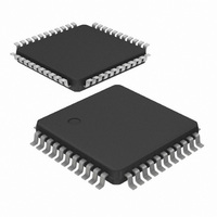
IC 80C51 MCU 16K OTP 44-LQFP
Manufacturer
NXP Semiconductors
Series
87Cr
Datasheet
1.P87C660X2BBD157.pdf
(102 pages)
Specifications of P87C660X2BBD,157
Core Processor
8051
Core Size
8-Bit
Speed
33MHz
Connectivity
EBI/EMI, I²C, UART/USART
Peripherals
POR, PWM, WDT
Number Of I /o
32
Program Memory Size
16KB (16K x 8)
Program Memory Type
OTP
Ram Size
512 x 8
Voltage - Supply (vcc/vdd)
2.7 V ~ 5.5 V
Oscillator Type
Internal
Operating Temperature
0°C ~ 70°C
Package / Case
44-LQFP
Processor Series
P87C6x
Core
80C51
Data Bus Width
8 bit
Data Ram Size
512 B
Interface Type
I2C, UART
Maximum Clock Frequency
16 MHz, 33 MHz
Number Of Programmable I/os
32
Number Of Timers
3
Operating Supply Voltage
2.7 V to 5.5 V
Maximum Operating Temperature
+ 70 C
Mounting Style
SMD/SMT
3rd Party Development Tools
PK51, CA51, A51, ULINK2
Minimum Operating Temperature
0 C
Lead Free Status / RoHS Status
Lead free / RoHS Compliant
Eeprom Size
-
Data Converters
-
Lead Free Status / Rohs Status
Details
Other names
568-3204
935273061157
P87C660X2BBD
935273061157
P87C660X2BBD
Available stocks
Company
Part Number
Manufacturer
Quantity
Price
Company:

Part Number:
P87C660X2BBD,157
Manufacturer:
NXP Semiconductors
Quantity:
10 000


the Standard-mode, and yet, it is downward compatible with the
Philips Semiconductors
SIO1 and SIO2, I
The I
information between devices connected to the bus. The main
features of the bus are:
For more information see the Philips publication “The I
Specification”, especially for detailed descriptions of the Fast and
the Standard data-transfer modes. Also, refer to the data sheets for
the 8xC552, the 8xC554, the 8xC557, and the 8xC65x.
The SIO1 I
data-transfer mode, either the 400Kbit/s Fast-mode or the 100Kbit/s
Standard-mode. In the Fast-mode, the port performance and the
register definitions are identical to those of the 8xC557 devices, and
in the Standard-mode (the reset default), they are identical to those
of the 8xC652, 8xC654, 8xC552, and 8xC554 devices.
The Fast-mode is functionally the same as the Standard-mode
except for the bit rate selection (see Tables 7 and 8), the timing
of the SCL and SDA signals (see the I
characteristics), and the output slew-rate control. The
Fast-mode allows up to a four-fold bit-rate increase over that of
Standard-mode, i.e. it can be used in a 0 to 100Kbit/s bus
system.
The SCL serial port for the clock line of the I
function of the P1.6 port pin, and the SDA serial port for the data line
of the I
Consequently, these 2 port pins are open drain outputs (no
pull-ups), and the output latches of P1.6 and P1.7 must be set to
logic 1 in order to enable the SIO1 outputs.
The second I
400Kbit/s Fast data-transfer mode only and selectable slew-rate
control of the output pins. It also has the same port performance
and register definitions as those of the 8xC557. The SCL1 and
SDA1 serial ports have dedicated pins with open-drain outputs and
Schmitt-trigger inputs.
There is an analog circuit for controlling the turn-on and turn-off
rates of the output pull-down (slew-rate control circuit) which is
required to meet the electrical specifications of the Fast-mode under
nominal conditions (5 V). To achieve the maximum slew-rates, the
2003 Oct 02
Only two bus lines are required: a serial clock line (SCL) and a
serial data line (SDA).
Bi-directional data transfer between masters and slaves.
Each device connected to the bus is software addressable by a
unique address.
Masters can operate as Master-transmitter or as Master-receiver.
It is a true multi-master bus (no central master) and includes
collision detection and arbitration to prevent data corruption if two
or more masters simultaneously initiate data transfer.
Serial clock synchronization allows devices with different bit rates
to communicate via the same serial bus.
Serial clock synchronization can be used as a handshake
mechanism to suspend and resume serial transfer.
Devices can be added to or removed from an I
without affecting any other device on the bus.
Fault diagnostics and debugging are simple; malfunctions can be
immediately traced.
80C51 8-bit microcontroller family
RAM, low voltage (2.7 to 5.5 V), low power, high speed (30/33
MHz), two 400KB I
2
C-bus is a simple bi-directional 2-wire bus to transfer
2
C bus is an alternate function of the P1.7 port pin.
2
C serial port interface has a selectable bi-directional
2
C serial port of the 8xC661X2, SIO2, has the
2
C Serial I/O
2
C interfaces
2
C electrical
2
C bus is an alternate
16 KB OTP/ROM, 512B
2
C-bus system
2
C-Bus
31
on the state of the direction bit (R/W), two types of data transfers are
circuit must be disabled. For the SIO1 serial port, the slew-rate
control circuits for both the SCL and SDA pins are disabled in the
Standard mode (maximum slew-rate), and they are enabled in the
Fast-mode. For the SIO2 serial port, the slew-rate control circuits
for both pins are enabled by reset, but the Slew-Rate Disable bit
(SRD bit) in the AUXR Register disables the slew-rate circuits for
both the SCL1 and SDA1 pins when set for maximum slew-rates.
This feature of the SIO2 slew-rate control is very useful for higher
bus loads, higher temperatures and lower voltages that cause
additional decreases in slew-rates.
All of the functional descriptions discussed below apply to
both the SIO1 and the SIO2 I
may refer to the SIO1 only. See page 10 for the corresponding
SIO2 register addresses.
The I
generation, address recognition and bus control arbitration, and
interfaces to the external I
SDA. It meets the I
modes (other than the low-speed mode) from-and-to the I
The logic handles byte transfers autonomously. It also keeps track
of serial transfers, and a status register (SxSTA) reflects the status
of the SIOx logic and the I
The CPU interfaces to the logic of each of the two I
following four Special Function Registers (where x=1,2):
A typical I
shows how a data transfer is accomplished on the bus. Depending
possible on the I
1. Data transfer from a master transmitter to a slave receiver. The
2. Data transfer from a slave transmitter to a master receiver. The
The master device generates all of the serial clock pulses and the
START and STOP conditions. A transfer is ended with a STOP
condition or with a repeated START condition. Since a repeated
START condition is also the beginning of the next serial transfer, the
I
Modes of Operation: The on-chip SIO1 logic may operate in the
following four modes:
1. Master Transmitter Mode:
2
C bus will not be released.
SxCON: Control register, bit addressable by the CPU.
SxSTA: Status register whose contents may be used as a vector
to service routines.
SxDAT: Data shift register; the data byte is stable as long as the
SI bit = 1 (SxCON.3).
SxADR: Slave address register; its LSB enables / disables
general call address recognition.
first byte transmitted by the master is the slave address. Next
follows a number of data bytes. The slave returns an
acknowledge bit after each received byte.
first byte (the slave address) is transmitted by the master. The
slave then returns an acknowledge bit. Next follows the data
bytes transmitted by the slave to the master. The master returns
an acknowledge bit after all received bytes other than the last
byte. At the end of the last received byte, a “not acknowledge” is
returned.
Serial data output through P1.7/SDA while P1.6/SCL outputs the
serial clock. The first byte transmitted contains the slave address
2
C on-chip logic performs a byte oriented data transfer, clock
2
C-bus configuration is shown in Figure 15, and Figure 16
2
C-bus:
2
C-bus specification and supports all transfer
2
2
C-bus via the two port pins SCL and
C-bus.
2
C serial ports although the text
P8xC660X2/661X2
2
Cs via the
Product data
2
C-bus.
Related parts for P87C660X2BBD,157
Image
Part Number
Description
Manufacturer
Datasheet
Request
R

Part Number:
Description:
80C51 8-bit microcontroller family
Manufacturer:
PHILIPS [NXP Semiconductors]
Datasheet:

Part Number:
Description:
NXP Semiconductors designed the LPC2420/2460 microcontroller around a 16-bit/32-bitARM7TDMI-S CPU core with real-time debug interfaces that include both JTAG andembedded trace
Manufacturer:
NXP Semiconductors
Datasheet:

Part Number:
Description:
NXP Semiconductors designed the LPC2458 microcontroller around a 16-bit/32-bitARM7TDMI-S CPU core with real-time debug interfaces that include both JTAG andembedded trace
Manufacturer:
NXP Semiconductors
Datasheet:
Part Number:
Description:
NXP Semiconductors designed the LPC2468 microcontroller around a 16-bit/32-bitARM7TDMI-S CPU core with real-time debug interfaces that include both JTAG andembedded trace
Manufacturer:
NXP Semiconductors
Datasheet:
Part Number:
Description:
NXP Semiconductors designed the LPC2470 microcontroller, powered by theARM7TDMI-S core, to be a highly integrated microcontroller for a wide range ofapplications that require advanced communications and high quality graphic displays
Manufacturer:
NXP Semiconductors
Datasheet:
Part Number:
Description:
NXP Semiconductors designed the LPC2478 microcontroller, powered by theARM7TDMI-S core, to be a highly integrated microcontroller for a wide range ofapplications that require advanced communications and high quality graphic displays
Manufacturer:
NXP Semiconductors
Datasheet:
Part Number:
Description:
The Philips Semiconductors XA (eXtended Architecture) family of 16-bit single-chip microcontrollers is powerful enough to easily handle the requirements of high performance embedded applications, yet inexpensive enough to compete in the market for hi
Manufacturer:
NXP Semiconductors
Datasheet:
Part Number:
Description:
The XA-S3 device is a member of Philips Semiconductors? XA(eXtended Architecture) family of high performance 16-bitsingle-chip microcontrollers
Manufacturer:
NXP Semiconductors
Datasheet:

Part Number:
Description:
The NXP BlueStreak LH75401/LH75411 family consists of two low-cost 16/32-bit System-on-Chip (SoC) devices
Manufacturer:
NXP Semiconductors
Datasheet:
Part Number:
Description:
The NXP LPC3130/3131 combine an 180 MHz ARM926EJ-S CPU core, high-speed USB2
Manufacturer:
NXP Semiconductors
Datasheet:
Part Number:
Description:
The NXP LPC3141 combine a 270 MHz ARM926EJ-S CPU core, High-speed USB 2
Manufacturer:
NXP Semiconductors
Part Number:
Description:
The NXP LPC3143 combine a 270 MHz ARM926EJ-S CPU core, High-speed USB 2
Manufacturer:
NXP Semiconductors

Part Number:
Description:
The NXP LPC3152 combines an 180 MHz ARM926EJ-S CPU core, High-speed USB 2
Manufacturer:
NXP Semiconductors
Part Number:
Description:
The NXP LPC3154 combines an 180 MHz ARM926EJ-S CPU core, High-speed USB 2
Manufacturer:
NXP Semiconductors