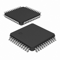
P87C660X2BBD,157 NXP Semiconductors, P87C660X2BBD,157 Datasheet - Page 75

P87C660X2BBD,157
Manufacturer Part Number
P87C660X2BBD,157
Description
IC 80C51 MCU 16K OTP 44-LQFP
Manufacturer
NXP Semiconductors
Series
87Cr
Datasheet
1.P87C660X2BBD157.pdf
(102 pages)
Specifications of P87C660X2BBD,157
Core Processor
8051
Core Size
8-Bit
Speed
33MHz
Connectivity
EBI/EMI, I²C, UART/USART
Peripherals
POR, PWM, WDT
Number Of I /o
32
Program Memory Size
16KB (16K x 8)
Program Memory Type
OTP
Ram Size
512 x 8
Voltage - Supply (vcc/vdd)
2.7 V ~ 5.5 V
Oscillator Type
Internal
Operating Temperature
0°C ~ 70°C
Package / Case
44-LQFP
Processor Series
P87C6x
Core
80C51
Data Bus Width
8 bit
Data Ram Size
512 B
Interface Type
I2C, UART
Maximum Clock Frequency
16 MHz, 33 MHz
Number Of Programmable I/os
32
Number Of Timers
3
Operating Supply Voltage
2.7 V to 5.5 V
Maximum Operating Temperature
+ 70 C
Mounting Style
SMD/SMT
3rd Party Development Tools
PK51, CA51, A51, ULINK2
Minimum Operating Temperature
0 C
Lead Free Status / RoHS Status
Lead free / RoHS Compliant
Eeprom Size
-
Data Converters
-
Lead Free Status / Rohs Status
Details
Other names
568-3204
935273061157
P87C660X2BBD
935273061157
P87C660X2BBD
Available stocks
Company
Part Number
Manufacturer
Quantity
Price
Company:
Part Number:
P87C660X2BBD,157
Manufacturer:
NXP Semiconductors
Quantity:
10 000
Philips Semiconductors
Expanded Data RAM Addressing
The P8xC660X2/661X2 has internal data memory that is mapped
into four separate segments: the lower 128 bytes of RAM, upper 128
bytes of RAM, 128 bytes Special Function Register (SFR), and
256 bytes expanded RAM (ERAM) (768 bytes for the RD2).
The four segments are:
1. The Lower 128 bytes of RAM (addresses 00H to 7FH) are
2. The Upper 128 bytes of RAM (addresses 80H to FFH) are
3. The Special Function Registers, SFRs, (addresses 80H to FFH)
4. The 256/768-bytes expanded RAM (ERAM, 00H – 1FFH/2FFH)
The Lower 128 bytes can be accessed by either direct or indirect
addressing. The Upper 128 bytes can be accessed by indirect
addressing only. The Upper 128 bytes occupy the same address
space as the SFR. That means they have the same address, but are
physically separate from SFR space.
When an instruction accesses an internal location above address
7FH, the CPU knows whether the access is to the upper 128 bytes
of data RAM or to SFR space by the addressing mode used in the
instruction. Instructions that use direct addressing access SFR
space. For example:
accesses the SFR at location 0A0H (which is P2). Instructions that
use indirect addressing access the Upper 128 bytes of data RAM.
2003 Oct 02
80C51 8-bit microcontroller family
RAM, low voltage (2.7 to 5.5 V), low power, high speed (30/33
MHz), two 400KB I
MOV 0A0H,#data
directly and indirectly addressable.
indirectly addressable only.
are directly addressable only.
are indirectly accessed by move external instruction, MOVX, and
with the EXTRAM bit cleared, see Figure 48.
2
C interfaces
16 KB OTP/ROM, 512B
75
For example:
where R0 contains 0A0H, accesses the data byte at address 0A0H,
rather than P2 (whose address is 0A0H).
The ERAM can be accessed by indirect addressing, with EXTRAM
bit cleared and MOVX instructions. This part of memory is physically
located on-chip, logically occupies the first 256/768 bytes of external
data memory in the P8xC660X2/661X2.
With EXTRAM = 0, the ERAM is indirectly addressed, using the
MOVX instruction in combination with any of the registers R0, R1 of
the selected bank or DPTR. An access to ERAM will not affect ports
P0, P3.6 (WR#) and P3.7 (RD#). P2 SFR is output during external
addressing. For example, with EXTRAM = 0,
where R0 contains 0A0H, accesses the ERAM at address 0A0H
rather than external memory. An access to external data memory
locations higher than the ERAM will be performed with the MOVX
DPTR instructions in the same way as in the standard 80C51, so
with P0 and P2 as data/address bus, and P3.6 and P3.7 as write
and read timing signals. Refer to Figure 49.
With EXTRAM = 1, MOVX @Ri and MOVX @DPTR will be similar
to the standard 80C51. MOVX @ Ri will provide an 8-bit address
multiplexed with data on Port 0 and any output port pins can be
used to output higher order address bits. This is to provide the
external paging capability. MOVX @DPTR will generate a 16-bit
address. Port 2 outputs the high-order eight address bits (the
contents of DPH) while Port 0 multiplexes the low-order eight
address bits (DPL) with data. MOVX @Ri and MOVX @DPTR will
generate either read or write signals on P3.6 (WR) and P3.7 (RD).
The stack pointer (SP) may be located anywhere in the 256 bytes
RAM (lower and upper RAM) internal data memory. The stack may
not be located in the ERAM.
MOV @R0,acc
MOVX @R0,acc
P8xC660X2/661X2
Product data


