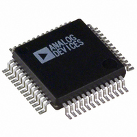
ADUC834BSZ Analog Devices Inc, ADUC834BSZ Datasheet - Page 21

ADUC834BSZ
Manufacturer Part Number
ADUC834BSZ
Description
IC ADC DUAL16/24BIT W/MCU 52MQFP
Manufacturer
Analog Devices Inc
Series
MicroConverter® ADuC8xxr
Specifications of ADUC834BSZ
Core Size
8-Bit
Program Memory Size
62KB (62K x 8)
Oscillator Type
Internal
Core Processor
8052
Speed
12.58MHz
Connectivity
EBI/EMI, I²C, SPI, UART/USART
Peripherals
POR, PSM, PWM, Temp Sensor, WDT
Number Of I /o
34
Program Memory Type
FLASH
Eeprom Size
4K x 8
Ram Size
2.25K x 8
Voltage - Supply (vcc/vdd)
2.7 V ~ 5.25 V
Data Converters
A/D 3x16b, 4x24b; D/A 1x12b
Operating Temperature
-40°C ~ 125°C
Package / Case
52-MQFP, 52-PQFP
Controller Family/series
(8052) ADUC
No. Of I/o's
26
Eeprom Memory Size
62KB
Ram Memory Size
2KB
Cpu Speed
12.58MHz
Package
52MQFP
Device Core
8052
Family Name
ADuC8xx
Maximum Speed
12.58 MHz
Operating Supply Voltage
3.3|5 V
Data Bus Width
8 Bit
Number Of Programmable I/os
26
Interface Type
I2C/SPI/UART
On-chip Adc
4-chx16-bit|4-chx24-bit
On-chip Dac
1-chx12-bit
Number Of Timers
3
Lead Free Status / RoHS Status
Lead free / RoHS Compliant
Available stocks
Company
Part Number
Manufacturer
Quantity
Price
Company:
Part Number:
ADUC834BSZ
Manufacturer:
TOSHIBA
Quantity:
1 200
Company:
Part Number:
ADUC834BSZ
Manufacturer:
Analog Devices Inc
Quantity:
10 000
Part Number:
ADUC834BSZ
Manufacturer:
ADI/亚德诺
Quantity:
20 000
SF (Sinc Filter Register)
The number in this register sets the decimation factor and thus
the output update rate for the primary and auxiliary ADCs.
This SFR cannot be written by user software while either ADC
is active. The update rate applies to both primary and auxiliary
ADCs and is calculated as follows:
Where:
The allowable range for SF is 0DH to FFH. Examples of SF values
and corresponding conversion update rates (f
times (t
ICON (Current Sources Control Register)
Used to control and configure the various excitation and burnout current source options available on-chip.
SFR Address
Power-On Default Value
Bit Addressable
Bit
7
6
5
4
3
2
1
0
*Both current sources can be enabled to the same external pin, yielding a 400 A current source.
REV. A
ADC
) are shown in Table VIII. The power-on default
f
f
SF = Decimal Value of SF Register
ADC
MOD
Name
–––
BO
ADC1IC
ADC0IC
I2PIN*
I1PIN*
I2EN
I1EN
= ADC Output Update Rate
= Modulator Clock Frequency = 32.768 kHz
f
ADC
=
1
3
×
8
×
1
SF
D5H
00H
No
Description
Reserved for Future Use
Burnout Current Enable Bit.
Set by user to enable both transducer burnout current sources in the primary ADC signal paths.
Cleared by user to disable both transducer burnout current sources.
Auxiliary ADC Current Correction Bit.
Set by user to allow scaling of the auxiliary ADC by an internal current source calibration word.
Primary ADC Current Correction Bit.
Set by user to allow scaling of the primary ADC by an internal current source calibration word.
Current Source-2 Pin Select Bit.
Set by user to enable current source-2 (200 A) to external Pin 3 (P1.2/DAC/IEXC1).
Cleared by user to enable current source-2 (200 A) to external Pin 4 (P1.3/AIN5/IEXC2).
Current Source-1 Pin Select Bit.
Set by user to enable current source-1 (200 A) to external Pin 4 (P1.3/AIN5/IEXC2).
Cleared by user to enable current source-1 (200 A) to external Pin 3 (P1.2/DAC/IEXC1).
Current Source-2 Enable Bit.
Set by user to turn on excitation current source-2 (200 A).
Cleared by user to turn off excitation current source-2 (200 A).
Current Source-1 Enable Bit.
Set by user to turn on excitation current source-1 (200 A).
Cleared by user to turn off excitation current source-1 (200 A).
×
f
MOD
ADC
Table IX. ICON SFR Bit Designations
) and conversion
–21–
value for the SF Register is 45H, resulting in a default ADC
update rate of just under 20 Hz. Both ADC inputs are chopped
to minimize offset errors, which means that the settling time for
a single conversion, or the time to a first conversion result in
Continuous Conversion mode, is 2
all calibration cycles will be carried out automatically with a
maximum, i.e., FFH, SF value to ensure optimum calibration
performance. Once a calibration cycle has completed, the value
in the SF Register will be that programmed by user software.
SF(dec)
13
69
255
Table VIII. SF SFR Bit Designations
SF(hex)
0D
45
FF
f
105.3
19.79
5.35
ADC
t
ADC
(Hz)
. As mentioned earlier,
ADuC834
t
9.52
50.34
186.77
ADC
(ms)


