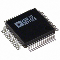
ADUC834BSZ Analog Devices Inc, ADUC834BSZ Datasheet - Page 33

ADUC834BSZ
Manufacturer Part Number
ADUC834BSZ
Description
IC ADC DUAL16/24BIT W/MCU 52MQFP
Manufacturer
Analog Devices Inc
Series
MicroConverter® ADuC8xxr
Specifications of ADUC834BSZ
Core Size
8-Bit
Program Memory Size
62KB (62K x 8)
Oscillator Type
Internal
Core Processor
8052
Speed
12.58MHz
Connectivity
EBI/EMI, I²C, SPI, UART/USART
Peripherals
POR, PSM, PWM, Temp Sensor, WDT
Number Of I /o
34
Program Memory Type
FLASH
Eeprom Size
4K x 8
Ram Size
2.25K x 8
Voltage - Supply (vcc/vdd)
2.7 V ~ 5.25 V
Data Converters
A/D 3x16b, 4x24b; D/A 1x12b
Operating Temperature
-40°C ~ 125°C
Package / Case
52-MQFP, 52-PQFP
Controller Family/series
(8052) ADUC
No. Of I/o's
26
Eeprom Memory Size
62KB
Ram Memory Size
2KB
Cpu Speed
12.58MHz
Package
52MQFP
Device Core
8052
Family Name
ADuC8xx
Maximum Speed
12.58 MHz
Operating Supply Voltage
3.3|5 V
Data Bus Width
8 Bit
Number Of Programmable I/os
26
Interface Type
I2C/SPI/UART
On-chip Adc
4-chx16-bit|4-chx24-bit
On-chip Dac
1-chx12-bit
Number Of Timers
3
Lead Free Status / RoHS Status
Lead free / RoHS Compliant
Available stocks
Company
Part Number
Manufacturer
Quantity
Price
Company:
Part Number:
ADUC834BSZ
Manufacturer:
TOSHIBA
Quantity:
1 200
Company:
Part Number:
ADUC834BSZ
Manufacturer:
Analog Devices Inc
Quantity:
10 000
Part Number:
ADUC834BSZ
Manufacturer:
ADI/亚德诺
Quantity:
20 000
Programming the Flash/EE Data Memory
A user wishes to program F3H into the second byte on Page 03H
of the Flash/EE data memory space while preserving the other
three bytes already in this page.
A typical program of the Flash/EE data array will involve:
Step 1: Set Up the Page Address
The two address registers EADRH and EADRL hold the high
byte address and the low byte address of the page to be addressed.
The assembly language to set up the address may appear as:
Step 2: Set Up the EDATA Registers
The four values to be written into the page into the 4 SFRs
EDATA1–4. Unfortunately we do not know three of them. Thus it
is necessary to read the current page and overwrite the second byte.
Step 3: Program Page
A byte in the Flash/EE array can only be programmed if it has
previously been erased. To be more specific, a byte can only be
programmed if it already holds the value FFH. Because of the
Flash/EE architecture, this erase must happen at a page level.
Therefore, a minimum of 4 bytes (1 page) will be erased when
an erase command is initiated. Once the page is erased, we can
program the 4 bytes in-page and then perform a verification of
the data.
REV. A
1. setting EADRH/L with the page address
2. writing the data to be programmed to the EDATA1–4
3. writing the ECON SFR with the appropriate command
MOV
MOV
MOV
MOV
MOV ECON,#5
MOV ECON,#2
MOV ECON,#4
MOV A,ECON
JNZ ERROR
ECON,#1
EADRH,#0
EADRL,#03H
EDATA2,#0F3H ;
;
;
;
;
;
Set Page Address Pointer
;
ERASE Page
WRITE Page
VERIFY Page
Check if ECON=0 (OK!)
Read Page into EDATA1-4
Overwrite byte 2
–33–
Note: although the 4 Kbytes of Flash/EE data memory is shipped
from the factory pre-erased, i.e., Byte locations set to FFH, it is
nonetheless good programming practice to include an erase-all
routine as part of any configuration/setup code running on the
ADuC834. An “ERASE-ALL” command consists of writing
“06H” to the ECON SFR, which initiates an erase of the 4-Kbyte
Flash/EE array. This command coded in 8051 assembly would
appear as:
Flash/EE Memory Timing
Typical program and erase times for the ADuC834 are as follows:
Normal Mode (operating on Flash/EE data memory)
ULOAD Mode (operating on Flash/EE program memory)
It should be noted that a given mode of operation is initiated as
soon as the command word is written to the ECON SFR. The
core microcontroller operation on the ADuC834 is idled until
the requested Program/Read or Erase mode is completed.
In practice, this means that even though the Flash/EE memory
mode of operation is typically initiated with a two-machine cycle
MOV instruction (to write to the ECON SFR), the next instruction
will not be executed until the Flash/EE operation is complete.
This means that the core will not respond to interrupt requests
until the Flash/EE operation is complete, although the core
peripheral functions like Counter/Timers will continue to count
and time as configured throughout this period.
MOV ECON,#06H
READPAGE (4 bytes)
WRITEPAGE (4 bytes)
VERIFYPAGE (4 bytes)
ERASEPAGE (4 bytes)
ERASEALL (4 Kbytes)
READBYTE (1 byte)
WRITEBYTE (1 byte)
WRITEPAGE (256 bytes)
ERASEPAGE (64 bytes)
ERASEALL (56 Kbytes)
WRITEBYTE (1 byte)
;
;
2 ms Duration
Erase all Command
– 5 machine cycles
– 380 s
– 5 machine cycles
– 2 ms
– 2 ms
– 3 machine cycles
– 200 s
– 15 ms
– 2 ms
– 2 ms
– 200 s
ADuC834


