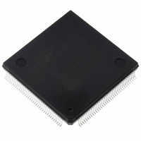
ST10F269Z2Q3 STMicroelectronics, ST10F269Z2Q3 Datasheet - Page 83

ST10F269Z2Q3
Manufacturer Part Number
ST10F269Z2Q3
Description
IC FLASH MEM 256KBIT 144-PQFP
Manufacturer
STMicroelectronics
Series
ST10r
Datasheet
1.ST10F269Z2Q3.pdf
(184 pages)
Specifications of ST10F269Z2Q3
Core Processor
ST10
Core Size
16-Bit
Speed
40MHz
Connectivity
CAN, EBI/EMI, SSC, UART/USART
Peripherals
POR, PWM, WDT
Number Of I /o
111
Program Memory Size
256KB (256K x 8)
Program Memory Type
FLASH
Ram Size
12K x 8
Voltage - Supply (vcc/vdd)
4.5 V ~ 5.5 V
Data Converters
A/D 16x10b
Oscillator Type
Internal
Operating Temperature
-40°C ~ 125°C
Package / Case
144-QFP
Processor Series
ST10F26x
Core
ST10
Data Bus Width
16 bit
Data Ram Size
12 KB
Interface Type
CAN, SSC, USART
Maximum Clock Frequency
40 MHz
Number Of Programmable I/os
111
Number Of Timers
2 x 16 bit
Operating Supply Voltage
0.3 V to 4 V
Maximum Operating Temperature
+ 125 C
Mounting Style
SMD/SMT
Minimum Operating Temperature
- 40 C
On-chip Adc
16 bit x 10 bit
Cpu Family
ST10
Device Core Size
16b
Frequency (max)
40MHz
Total Internal Ram Size
12KB
# I/os (max)
111
Number Of Timers - General Purpose
5
Operating Supply Voltage (typ)
5V
Operating Supply Voltage (max)
5.5V
Operating Supply Voltage (min)
4.5V
Instruction Set Architecture
CISC/RISC
Operating Temp Range
-40C to 125C
Operating Temperature Classification
Automotive
Mounting
Surface Mount
Pin Count
144
Package Type
PQFP
Lead Free Status / RoHS Status
Lead free / RoHS Compliant
Eeprom Size
-
Lead Free Status / Rohs Status
Lead free / RoHS Compliant
Other names
497-2042
Available stocks
Company
Part Number
Manufacturer
Quantity
Price
Company:
Part Number:
ST10F269Z2Q3
Manufacturer:
INFINEON
Quantity:
1 443
Company:
Part Number:
ST10F269Z2Q3
Manufacturer:
STMicroelectronics
Quantity:
10 000
Part Number:
ST10F269Z2Q3
Manufacturer:
ST
Quantity:
20 000
ST10F269
ODP6 (F1CEH / E7H)
12.9.1 - Alternate Functions of Port 6
A programmable number of chip select signals (CS4...CS0) derived from the bus control registers
(BUSCON4...BUSCON0) can be output on 5 pins of Port 6.
The number of chip select signals is selected via PORT0 during reset. The selected value can be read
from bit-field CSSEL in register RP0H (read only) in order to check the configuration during run time.
The Table 23 summarizes the alternate functions of Port 6 depending on the number of selected chip
select lines (coded via bit-field CSSEL).
Table 23 : Port 6 Alternate Functions
Figure 36 : Port 6 I/O and Alternate Functions
DP6.y
ODP6.y
15
-
Port 6
P6.0
P6.1
P6.2
P6.3
P6.4
P6.5
P6.6
P6.7
14
-
13
-
HOLD External hold request input
HLDA Hold acknowledge output
BREQ Bus request output
General purpose I/O
General purpose I/O
General purpose I/O
General purpose I/O
General purpose I/O
Alternate Function
12
Port Direction Register DP6 Bit y
DP6.y = 0: Port line P6.y is an input (high impedance)
DP6.y = 1: Port line P6.y is an output
Port 6 Open Drain Control Register Bit y
ODP6.y = 0: Port line P6.y output driver in push-pull mode
ODP6.y = 1: Port line P6.y output driver in open drain mode
-
CSSEL = 10
General Purpose Input/Output
11
Port 6
-
Alternate Function
10
-
9
-
P6.7
P6.6
P6.5
P6.4
P6.3
P6.2
P6.1
P6.0
8
General purpose I/O
General purpose I/O
General purpose I/O
-
Alternate Function
Chip select CS0
Chip select CS1
CSSEL = 01
ODP6.7 ODP6.6 ODP6.5 ODP6.4 ODP6.3 ODP6.2 ODP6.1 ODP6.0
RW
7
ESFR
RW
6
RW
5
General purpose I/O
General purpose I/O
Alternate Function
Chip select CS0
Chip select CS1
Chip select CS2
CSSEL = 00
RW
4
a)
BREQ
HLDA
HOLD
CS4
CS3
CS2
CS1
CS0
RW
12 - PARALLEL PORTS
3
RW
2
Alternate Function
Chip select CS0
Chip select CS1
Chip select CS2
Chip select CS3
Chip select CS4
Reset Value: --00h
CSSEL = 11
RW
1
83/184
RW
0


