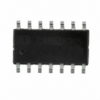
C8051F305-GS Silicon Laboratories Inc, C8051F305-GS Datasheet - Page 104

C8051F305-GS
Manufacturer Part Number
C8051F305-GS
Description
IC 8051 MCU 2K FLASH 14-SOIC
Manufacturer
Silicon Laboratories Inc
Series
C8051F30xr
Specifications of C8051F305-GS
Program Memory Type
FLASH
Program Memory Size
2KB (2K x 8)
Package / Case
14-SOIC (3.9mm Width), 14-SOL
Core Processor
8051
Core Size
8-Bit
Speed
25MHz
Connectivity
SMBus (2-Wire/I²C), UART/USART
Peripherals
POR, PWM, WDT
Number Of I /o
8
Ram Size
256 x 8
Voltage - Supply (vcc/vdd)
2.7 V ~ 3.6 V
Oscillator Type
External
Operating Temperature
-40°C ~ 85°C
Processor Series
C8051F3x
Core
8051
Data Bus Width
8 bit
Data Ram Size
256 B
Interface Type
I2C/SMBus/UART
Maximum Clock Frequency
25 MHz
Number Of Programmable I/os
8
Number Of Timers
3
Maximum Operating Temperature
+ 85 C
Mounting Style
SMD/SMT
3rd Party Development Tools
PK51, CA51, A51, ULINK2
Development Tools By Supplier
C8051F300DK
Minimum Operating Temperature
- 40 C
Lead Free Status / RoHS Status
Lead free / RoHS Compliant
For Use With
770-1006 - ISP 4PORT FOR SILABS C8051F MCU336-1444 - ADAPTER PROGRAM TOOLSTICK F300
Eeprom Size
-
Data Converters
-
Lead Free Status / Rohs Status
Lead free / RoHS Compliant
Other names
336-1540-5
- Current page: 104 of 178
- Download datasheet (2Mb)
C8051F300/1/2/3/4/5
12.1. Priority Crossbar Decoder
The Priority Crossbar Decoder (Figure 12.3) assigns a priority to each I/O function, starting at the top with
UART0. When a digital resource is selected, the least significant unassigned Port pin is assigned to that
resource (excluding UART0, which is always at pins 4 and 5). If a Port pin is assigned, the Crossbar skips
that pin when assigning the next selected resource. Additionally, the Crossbar will skip Port pins whose
associated bits in the XBR0 register are set. The XBR0 register allows software to skip Port pins that are to
be used for analog input or GPIO.
Important Note on Crossbar Configuration: If a Port pin is claimed by a peripheral without use of the
Crossbar, its corresponding XBR0 bit should be set. This applies to P0.0 if VREF is enabled, P0.3 and/or
P0.2 if the external oscillator circuit is enabled, P0.6 if the ADC is configured to use the external conversion
start signal (CNVSTR), and any selected ADC or Comparator inputs. The Crossbar skips selected pins as
if they were already assigned, and moves to the next unassigned pin. Figure 12.3 shows the Crossbar
Decoder priority with no Port pins skipped (XBR0 = 0x00); Figure 12.4 shows the Crossbar Decoder prior-
ity with pins 6 and 2 skipped (XBR0 = 0x44).
104
Figure 12.3. Crossbar Priority Decoder with XBR0 = 0x00
SF Signals
PIN I/O
TX0
RX0
SDA
SCL
CP0
CP0A
SYSCLK
CEX0
CEX1
CEX2
ECI
T0
T1
SF Signals
VREF
Port pin potentially available to peripheral
Special Function Signals are not assigned by the crossbar.
When these signals are enabled, the CrossBar must be
manually configured to skip their corresponding port pins.
Note: x1 refers to the XTAL1 signal; x2 refers to the XTAL2
signal.
0
0
1
0
x1
2
0
XBR0[0:7]
x2
3
0
Rev. 2.9
P0
4
0
5
0
CNVSTR
6
0
7
0
Related parts for C8051F305-GS
Image
Part Number
Description
Manufacturer
Datasheet
Request
R
Part Number:
Description:
SMD/C°/SINGLE-ENDED OUTPUT SILICON OSCILLATOR
Manufacturer:
Silicon Laboratories Inc
Part Number:
Description:
Manufacturer:
Silicon Laboratories Inc
Datasheet:
Part Number:
Description:
N/A N/A/SI4010 AES KEYFOB DEMO WITH LCD RX
Manufacturer:
Silicon Laboratories Inc
Datasheet:
Part Number:
Description:
N/A N/A/SI4010 SIMPLIFIED KEY FOB DEMO WITH LED RX
Manufacturer:
Silicon Laboratories Inc
Datasheet:
Part Number:
Description:
N/A/-40 TO 85 OC/EZLINK MODULE; F930/4432 HIGH BAND (REV E/B1)
Manufacturer:
Silicon Laboratories Inc
Part Number:
Description:
EZLink Module; F930/4432 Low Band (rev e/B1)
Manufacturer:
Silicon Laboratories Inc
Part Number:
Description:
I°/4460 10 DBM RADIO TEST CARD 434 MHZ
Manufacturer:
Silicon Laboratories Inc
Part Number:
Description:
I°/4461 14 DBM RADIO TEST CARD 868 MHZ
Manufacturer:
Silicon Laboratories Inc
Part Number:
Description:
I°/4463 20 DBM RFSWITCH RADIO TEST CARD 460 MHZ
Manufacturer:
Silicon Laboratories Inc
Part Number:
Description:
I°/4463 20 DBM RADIO TEST CARD 868 MHZ
Manufacturer:
Silicon Laboratories Inc
Part Number:
Description:
I°/4463 27 DBM RADIO TEST CARD 868 MHZ
Manufacturer:
Silicon Laboratories Inc
Part Number:
Description:
I°/4463 SKYWORKS 30 DBM RADIO TEST CARD 915 MHZ
Manufacturer:
Silicon Laboratories Inc
Part Number:
Description:
N/A N/A/-40 TO 85 OC/4463 RFMD 30 DBM RADIO TEST CARD 915 MHZ
Manufacturer:
Silicon Laboratories Inc
Part Number:
Description:
I°/4463 20 DBM RADIO TEST CARD 169 MHZ
Manufacturer:
Silicon Laboratories Inc


