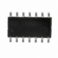
C8051F305-GS Silicon Laboratories Inc, C8051F305-GS Datasheet - Page 108

C8051F305-GS
Manufacturer Part Number
C8051F305-GS
Description
IC 8051 MCU 2K FLASH 14-SOIC
Manufacturer
Silicon Laboratories Inc
Series
C8051F30xr
Specifications of C8051F305-GS
Program Memory Type
FLASH
Program Memory Size
2KB (2K x 8)
Package / Case
14-SOIC (3.9mm Width), 14-SOL
Core Processor
8051
Core Size
8-Bit
Speed
25MHz
Connectivity
SMBus (2-Wire/I²C), UART/USART
Peripherals
POR, PWM, WDT
Number Of I /o
8
Ram Size
256 x 8
Voltage - Supply (vcc/vdd)
2.7 V ~ 3.6 V
Oscillator Type
External
Operating Temperature
-40°C ~ 85°C
Processor Series
C8051F3x
Core
8051
Data Bus Width
8 bit
Data Ram Size
256 B
Interface Type
I2C/SMBus/UART
Maximum Clock Frequency
25 MHz
Number Of Programmable I/os
8
Number Of Timers
3
Maximum Operating Temperature
+ 85 C
Mounting Style
SMD/SMT
3rd Party Development Tools
PK51, CA51, A51, ULINK2
Development Tools By Supplier
C8051F300DK
Minimum Operating Temperature
- 40 C
Lead Free Status / RoHS Status
Lead free / RoHS Compliant
For Use With
770-1006 - ISP 4PORT FOR SILABS C8051F MCU336-1444 - ADAPTER PROGRAM TOOLSTICK F300
Eeprom Size
-
Data Converters
-
Lead Free Status / Rohs Status
Lead free / RoHS Compliant
Other names
336-1540-5
- Current page: 108 of 178
- Download datasheet (2Mb)
C8051F300/1/2/3/4/5
12.3. General Purpose Port I/O
Port pins that remain unassigned by the Crossbar and are not used by analog peripherals can be used for
general purpose I/O. Port0 is accessed through a corresponding special function register (SFR) that is
both byte addressable and bit addressable. When writing to a Port, the value written to the SFR is latched
to maintain the output data value at each pin. When reading, the logic levels of the Port's input pins are
returned regardless of the XBRn settings (i.e., even when the pin is assigned to another signal by the
Crossbar, the Port register can always read its corresponding Port I/O pin). The exception to this is the
execution of the read-modify-write instructions. The read-modify-write instructions when operating on a
Port SFR are the following: ANL, ORL, XRL, JBC, CPL, INC, DEC, DJNZ and MOV, CLR or SET, when the
destination is an individual bit in a Port SFR. For these instructions, the value of the register (not the pin) is
read, modified, and written back to the SFR.
108
Bit7:
Bit6:
Bits5–3: UNUSED: Read = 000b. Write = don’t care.
Bit2:
Bit1:
Bit0:
WEAKPUD XBARE
R/W
Bit7
WEAKPUD: Port I/O Weak Pull-up Disable.
0: Weak Pull-ups enabled (except for Ports whose I/O are configured as push-pull).
1: Weak Pull-ups disabled.
XBARE: Crossbar Enable.
0: Crossbar disabled.
1: Crossbar enabled.
T1E: T1 Enable.
0: T1 unavailable at Port pin.
1: T1 routed to Port pin.
T0E: T0 Enable.
0: T0 unavailable at Port pin.
1: T0 routed to Port pin.
ECIE: PCA0 Counter Input Enable.
0: ECI unavailable at Port pin.
1: ECI routed to Port pin.
SFR Definition 12.3. XBR2: Port I/O Crossbar Register 2
R/W
Bit6
R/W
Bit5
—
R/W
Bit4
—
Rev. 2.9
R/W
Bit3
—
T1E
R/W
Bit2
T0E
R/W
Bit1
ECIE
R/W
Bit0
SFR Address:
00000000
Reset Value
0xE3
Related parts for C8051F305-GS
Image
Part Number
Description
Manufacturer
Datasheet
Request
R
Part Number:
Description:
SMD/C°/SINGLE-ENDED OUTPUT SILICON OSCILLATOR
Manufacturer:
Silicon Laboratories Inc
Part Number:
Description:
Manufacturer:
Silicon Laboratories Inc
Datasheet:
Part Number:
Description:
N/A N/A/SI4010 AES KEYFOB DEMO WITH LCD RX
Manufacturer:
Silicon Laboratories Inc
Datasheet:
Part Number:
Description:
N/A N/A/SI4010 SIMPLIFIED KEY FOB DEMO WITH LED RX
Manufacturer:
Silicon Laboratories Inc
Datasheet:
Part Number:
Description:
N/A/-40 TO 85 OC/EZLINK MODULE; F930/4432 HIGH BAND (REV E/B1)
Manufacturer:
Silicon Laboratories Inc
Part Number:
Description:
EZLink Module; F930/4432 Low Band (rev e/B1)
Manufacturer:
Silicon Laboratories Inc
Part Number:
Description:
I°/4460 10 DBM RADIO TEST CARD 434 MHZ
Manufacturer:
Silicon Laboratories Inc
Part Number:
Description:
I°/4461 14 DBM RADIO TEST CARD 868 MHZ
Manufacturer:
Silicon Laboratories Inc
Part Number:
Description:
I°/4463 20 DBM RFSWITCH RADIO TEST CARD 460 MHZ
Manufacturer:
Silicon Laboratories Inc
Part Number:
Description:
I°/4463 20 DBM RADIO TEST CARD 868 MHZ
Manufacturer:
Silicon Laboratories Inc
Part Number:
Description:
I°/4463 27 DBM RADIO TEST CARD 868 MHZ
Manufacturer:
Silicon Laboratories Inc
Part Number:
Description:
I°/4463 SKYWORKS 30 DBM RADIO TEST CARD 915 MHZ
Manufacturer:
Silicon Laboratories Inc
Part Number:
Description:
N/A N/A/-40 TO 85 OC/4463 RFMD 30 DBM RADIO TEST CARD 915 MHZ
Manufacturer:
Silicon Laboratories Inc
Part Number:
Description:
I°/4463 20 DBM RADIO TEST CARD 169 MHZ
Manufacturer:
Silicon Laboratories Inc


