R5F21122FP#U0 Renesas Electronics America, R5F21122FP#U0 Datasheet
R5F21122FP#U0
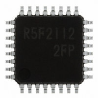
Specifications of R5F21122FP#U0
Available stocks


Related parts for R5F21122FP#U0


R5F21122FP#U0 Summary of contents
Page 1
To our customers, Old Company Name in Catalogs and Other Documents st On April 1 , 2010, NEC Electronics Corporation merged with Renesas Technology Corporation, and Renesas Electronics Corporation took over all the business of both companies. Therefore, although the ...
Page 2
All information included in this document is current as of the date this document is issued. Such information, however, is subject to change without any prior notice. Before purchasing or using any Renesas Electronics products listed herein, please confirm ...
Page 3
R8C/12 Group 16 Hardware Manual RENESAS 16-BIT SINGLE-CHIP MICROCOMPUTER M16C FAMILY / R8C /Tiny SERIES All information contained in these materials, including products and product specifications, represents information on the product at the time of publication and is subject to ...
Page 4
Keep safety first in your circuit designs! Renesas Technology Corp. puts the maximum effort into making semiconductor products 1. better and more reliable, but there is always the possibility that trouble may occur with them. Trouble with semiconductors may lead ...
Page 5
How to Use This Manual 1. Introduction This hardware manual provides detailed information on the R8C/12 Group of microcomputers. Users are expected to have basic knowledge of electric circuits, logical circuits and microcomputers. 2. Register Diagram The symbols, and descriptions, ...
Page 6
M16C Family Documents The following documents were prepared for the M16C family. Document Short Sheet Data Sheet Hardware Manual Software Manual Application Note RENESAS TECHNICAL UPDATE NOTES: 1. Before using this material, please visit the our website to verify ...
Page 7
Table of Contents SFR Page Reference Chapter 1. Overview ............................................................. 1 1.1 Applications ................................................................................................................... 1 1.2 Performance Overview .................................................................................................. 2 1.3 Block Diagram ............................................................................................................... 3 1.4 Product Information ...................................................................................................... 4 1.5 Pin Assignments ............................................................................................................ 5 1.6 Pin Description .............................................................................................................. 6 ...
Page 8
CPU Clock and Peripheral Function Clock ................................................................ 23 6.3.1 CPU Clock .............................................................................................................................................. 23 6.3.2 Peripheral Function Clock (f 6.3.3 f and f RING RING128 ................................................................................................................................................................... 6.4 Power Control ............................................................................................................... 24 6.4.1 Normal Operation Mode ....................................................................................................................... 24 6.4.2 Wait Mode ...
Page 9
Timer Z ........................................................................................................................... 73 12.3.1 Timer Mode .......................................................................................................................................... 76 12.3.2 Programmable Waveform Generation Mode .................................................................................... 78 12.3.3 Programmable One-shot Generation Mode ...................................................................................... 80 12.3.4 Programmable Wait One-shot Generation Mode ............................................................................. 83 12.4 Timer C ........................................................................................................................... 86 Chapter 13. Serial ...
Page 10
Standard Serial I/O Mode ......................................................................................... 158 17.5.1 ID Code Check Function .................................................................................................................. 158 Chapter 18. On-chip Debugger ........................................ 162 18.1 Address Match Interrupt .......................................................................................... 162 18.2 Single Step Interrupt ................................................................................................ 162 18.3 UART1 ........................................................................................................................ 162 18.4 BRK Instrucstion ...................................................................................................... ...
Page 11
SFR Page Reference ...
Page 12
SFR Page Reference ...
Page 13
R8C/12 Group SINGLE-CHIP 16-BIT CMOS MICROCOMPUTER 1. Overview This MCU is built using the high-performance silicon gate CMOS process using a R8C Tiny Series CPU core and is packaged in a 32-pin plastic molded LQFP. This MCU operates using sophisticated ...
Page 14
R8C/12 Group 1.2 Performance Overview Table 1.1. lists the performance outline of this MCU. Table 1.1 Performance outline Item CPU Number of basic instructions 89 instructions Minimum instruction execution time 62.5 ns (f(X Operating mode Address space Memory capacity Peripheral ...
Page 15
R8C/12 Group 1.3 Block Diagram Figure 1.1. shows this MCU block diagram ...
Page 16
R8C/12 Group 1.4 Product Information Table 1.2 lists the product information. Table 1.2 Product Information ROM capacity Type No. Program ROM 8K bytes R5F21122FP 12K bytes R5F21123FP R5F21124FP 16K bytes R5F21122DFP 8K bytes R5F21123DFP 12K bytes R5F21124DFP 16K bytes T ...
Page 17
R8C/12 Group 1.5 Pin Assignments Figure 1.3 shows the pin configuration (top view). PIN CONFIGURATION (top view / / ...
Page 18
R8C/12 Group 1.6 Pin Description Table 1.3 shows the pin description Table 1.3 Pin description Signal name Pin name Power supply Vcc, input Vss IVcc IVcc Analog power AVcc, supply input AVss ___________ Reset input RESET CNVss CNVss MODE MODE ...
Page 19
R8C/12 Group 2. Central Processing Unit (CPU) Figure 2.1 shows the CPU registers. The CPU has 13 registers. Of these, R0, R1, R2, R3, A0, A1 and FB comprise a register bank. Two sets of register banks are provided. b31 ...
Page 20
R8C/12 Group 2.2 Address Registers (A0 and A1 16-bit register for address register indirect addressing and address register relative addressing. They also are used for transfer, arithmetic and logic operations. The same applies A0. ...
Page 21
R8C/12 Group 3. Memory Figure 3 memory map of this MCU. This MCU provides 1-Mbyte address space from addresses 00000 to FFFFF . 16 16 The internal ROM (program ROM) is allocated lower addresses beginning with address 0FFFF ...
Page 22
R8C/12 Group 4. Special Function Register (SFR) SFR(Special Function Register) is the control register of peripheral functions. Tables 4.1 to 4.4 list the SFR information Table 4.1 SFR Information( ...
Page 23
R8C/12 Group Table 4.2 SFR Information( ...
Page 24
R8C/12 Group Table 4.3 SFR Information( ...
Page 25
R8C/12 Group Table 4.4 SFR Information( ...
Page 26
R8C/12 Group 5. Reset There are three types of resets: a hardware reset, a software reset, and an watchdog timer reset. 5.1 Hardware Reset A reset is applied using the RESET pin. When an “L” signal is applied to the ...
Page 27
R8C/12 Group b15 b19 Content of addresses 0FFFE b15 b15 b15 IPL Figure 5.1 CPU Register Status After Reset ...
Page 28
R8C/12 Group V RESET CC Figure 5.3 Example Reset Circuit RESET V CC Figure 5.4 Example Reset Circuit (Voltage Check Circuit) Rev.1.20 Jan 27, 2006 page 16 of 181 REJ09B0110-0120 2. RESET Supply ...
Page 29
R8C/12 Group 6. Clock Generation Circuit The clock generation circuit contains two oscillator circuits as follows: • Main clock oscillation circuit • On-chip oscillator (with oscillation stop detection function) Table 6.1 lists the clock generation circuit specifications. Figure 6.1 shows ...
Page 30
R8C/12 Group ...
Page 31
R8C/12 Group ...
Page 32
R8C/12 Group ...
Page 33
R8C/12 Group The following describes the clocks generated by the clock generation circuit. 6.1 Main Clock This clock is supplied by a main clock oscillation circuit. This clock is used as the clock source for the CPU and peripheral function ...
Page 34
R8C/12 Group 6.2 On-Chip Oscillator Clock This clock, approximately 125 kHz, is supplied by a on-chip oscillator. This clock is used as the clock source for the CPU clock, peripheral function clock, f After reset, the on-chip oscillator clock divided ...
Page 35
R8C/12 Group 6.3 CPU Clock and Peripheral Function Clock There are two types of clocks: CPU clock to operate the CPU and peripheral function clock to operate the peripheral functions. Also refer to “Figure 6.1 Clock Generating Circuit”. 6.3.1 CPU ...
Page 36
R8C/12 Group 6.4 Power Control There are three power control modes. All modes other than wait and stop modes are referred to as normal operation mode. 6.4.1 Normal Operation Mode Normal operation mode is further classified into three modes. In ...
Page 37
R8C/12 Group 6.4.2 Wait Mode In wait mode, the CPU clock is turned off, so are the CPU and the watchdog timer because both are operated by the CPU clock. Because the main clock and on-chip oscillator clock both are ...
Page 38
R8C/12 Group 6.4.3 Stop Mode In stop mode, all oscillator circuits are turned off, so are the CPU clock and the peripheral function clocks. Therefore, the CPU and the peripheral functions clocked by these clocks stop operating. The least amount ...
Page 39
R8C/12 Group Figure 6.5 shows the state transition of power control. On-chip Oscillator High-speed Mode, Middle-speed mode Interrupt WAIT Instruction Wait Mode Figure 6.5 State Transition of Power Control Rev.1.20 Jan 27, 2006 page 27 of 181 REJ09B0110-0120 Reset Mode ...
Page 40
R8C/12 Group 6.5 Oscillation Stop Detection Function The oscillation stop detection function is such that main clock oscillation circuit stop is detected. The oscillation stop detection function can be enabled and disabled by the OCD1 to OCD0 bits in the ...
Page 41
R8C/12 Group Table 6.5 Determination of Interrupt Factor of Oscillation Stop Detection or Watchdog Timer Interrupt) Generated Interrupt Factor Oscillation stop detection ( (a) or (b) ) Determine several times Set OCD1 to OCD0 bits to 00 (oscillation stop detection ...
Page 42
R8C/12 Group 7. Protection In the event that a program runs out of control, this function protects the important registers so that they will not be rewritten easily. Figure 7.1 shows the PRCR register. The following lists the registers protected ...
Page 43
R8C/12 Group 8. Processor Mode 8.1 Types of Processor Mode The processor mode is single-chip mode. Table 8.1 shows the features of the processor mode. Figure 8.1 shows the PM0 and PM1 register. Table 8.1 Features of Processor Mode Processor ...
Page 44
R8C/12 Group 9. Bus During access, the ROM/RAM and the SFR have different bus cycles. Table 9.1 shows bus cycles for access space. The ROM/RAM and SFR are connected to the CPU through an 8-bit bus. When accessing in word ...
Page 45
R8C/12 Group 10. Interrupt 10.1 Interrupt Overview 10.1.1 Type of Interrupts Figure 10.1 shows types of interrupts. Software (Non-maskable interrupt) Interrupt Hardware NOTES: 1. Peripheral function interrupts are generated by the peripheral functions built in the microcomputer system. 2. Avoid ...
Page 46
R8C/12 Group 10.1.2 Software Interrupts A software interrupt occurs when executing certain instructions. Software interrupts are non- maskable interrupts. • Undefined Instruction Interrupt An undefined instruction interrupt occurs when executing the UND instruction. • Overflow Interrupt An overflow interrupt occurs ...
Page 47
R8C/12 Group 10.1.3 Hardware Interrupts Hardware interrupts are classified into two types — special interrupts and peripheral function inter- rupts. (1) Special Interrupts Special interrupts are non-maskable interrupts. • Watchdog Timer Interrupt Generated by the watchdog timer. Once a watchdog ...
Page 48
R8C/12 Group 10.1.4 Interrupts and Interrupt Vector One interrupt vector consists of 4 bytes. Set the start address of each interrupt routine in the respec- tive interrupt vectors. When an interrupt request is accepted, the CPU branches to the address ...
Page 49
R8C/12 Group • Relocatable Vector Tables The 256 bytes beginning with the start address set in the INTB register comprise a relocatable vector table area. Table 10.2 lists interrupts and vector tables located in the relocatable vector table. Table 10.2 ...
Page 50
R8C/12 Group 10.1.5 Interrupt Control The following describes how to enable/disable the maskable interrupts, and how to set the priority in which order they are accepted. What is explained here does not apply to nonmaskable interrupts. Use the FLG register’s ...
Page 51
R8C/12 Group ...
Page 52
R8C/12 Group • I Flag The I flag enables or disables the maskable interrupt. Setting the I flag to “1” (enabled) enables the maskable interrupt. Setting the I flag to “0” (disabled) disables all maskable interrupts. • IR Bit The ...
Page 53
R8C/12 Group • Interrupt Sequence An interrupt sequence — what are performed over a period from the instant an interrupt is accepted to the instant the interrupt routine is executed — is described here interrupt occurs during execution ...
Page 54
R8C/12 Group • Interrupt Response Time Figure 10.5 shows the interrupt response time. The interrupt response or interrupt acknowledge time denotes a time from when an interrupt request is generated till when the first instruction in the inter- rupt routine ...
Page 55
R8C/12 Group • Saving Registers In the interrupt sequence, the FLG register and PC are saved to the stack. At this time, the 4 high-order bits in the PC and the 4 high-order (IPL) and 8 low-order bits in the ...
Page 56
R8C/12 Group • Returning from an Interrupt Routine The FLG register and PC in the state in which they were immediately before entering the interrupt sequence are restored from the stack by executing the REIT instruction at the end of ...
Page 57
R8C/12 Group • Interrupt Priority Resolution Circuit The interrupt priority resolution circuit is used to select the interrupt with the highest priority among those requested. Figure 10.9 shows the Interrupts Priority Select Circuit Priority level of each interrupt I N ...
Page 58
R8C/12 Group ______ 10.2 INT Interrupt ________ 10.2.1 INT0 Interrupt _______ INT0 interrupt is triggered by an INT0 input. When using INT0 interrupts, the INT0EN bit in the INTEN register must be set to “1” (enabling). The edge polarity is ...
Page 59
R8C/12 Group _______ 10.2.2 INT0 Input Filter _______ The INT0 input has a digital filter which can be sampled by one of three sampling clocks. The sampling clock is selected using the INT0F1 to INT0F0 bits in the INT0F register. ...
Page 60
R8C/12 Group ______ 10.2.3 INT1 Interrupt and INT2 Interrupt ______ INT1 interrupts are triggered by INT1 inputs. The edge polarity is selected with the R0EDG bit in the ______ TXMR register. The INT1 pin can be used only when the ...
Page 61
R8C/12 Group ______ 10.2.4 INT3 Interrupt _____ INT3 interrupts are triggered by INT3 inputs. The TCC07 bit in the TCC0 register should “0” ______ _______ (INT3). The INT3 input has a digital filter which can be sampled ...
Page 62
R8C/12 Group 10.3 Key Input Interrupt A key input interrupt is generated on an input edge of any of the K1 be used as a key-on wakeup function to exit wait or stop mode. KIi input can be enabled or ...
Page 63
R8C/12 Group 10.4 Address Match Interrupt An address match interrupt is generated immediately before executing the instruction at the address indicated by the RMADi register (i=0, 1). Set the start address of any instruction in the RMADi register. Use the ...
Page 64
R8C/12 Group Address match interrupt enable register Address match interrupt register (b19) (b16) (b15) (b23 Figure 10.17 AIER Register and RMAD0 to RMAD1 ...
Page 65
R8C/12 Group 11. Watchdog Timer The watchdog timer is the function of detecting when the program is out of control. Therefore, we recom- mend using the watchdog timer to improve reliability of a system. Figure 11.1 shows the watchdog timer ...
Page 66
R8C/12 Group ...
Page 67
R8C/12 Group 12. Timers The microcomputer has three 8-bit timers and one 16-bit timer. The three 8-bit timers are Timer X, Timer Y, and Timer Z and each one has an 8-bit prescaler. The 16-bit timer is Timer C and ...
Page 68
R8C/12 Group 12.1 Timer X The Timer 8-bit timer with an 8-bit prescaler. Figure 12.1 shows the block diagram of Timer X. Figures 12.2 and 12.3 show the Timer X-related registers. The Timer X has five operation ...
Page 69
R8C/12 Group Prescaler X Register b7 Timer X Register ...
Page 70
R8C/12 Group 12.1.1 Timer Mode In this mode, the timer counts an internally generated count source (See “Table 12.2 Timer Mode Specifications”). Figure 12.4 shows the TXMR register in timer mode. Table 12.2 Timer Mode Specifications Item Count source f ...
Page 71
R8C/12 Group 12.1.2 Pulse Output Mode In this mode, the timer counts an internally generated count source, and outputs from the CNTR0 pin a pulse whose polarity is inverted each time the timer underflows (See “Table 12.3 Pulse Output mode ...
Page 72
R8C/12 Group 12.1.3 Event Counter Mode In this mode, the timer counts an external signal fed to INT1/CNTR Counter Mode Specifications”). Figure 12.6 shows TXMR register in event counter mode. Table 12.4 Event Counter Mode Specifications Item Count source External ...
Page 73
R8C/12 Group 12.1.4 Pulse Width Measurement Mode In this mode, the timer measures the pulse width of an external signal fed to INT1/CNTR0 pin (See “Table 12.5 Pulse Width Measurement Mode Specifications”). Figure 12.7 shows the TXMR register in pulse ...
Page 74
R8C/12 Group n = high-level: the contents of TX register, low-level: the contents of PREX register FFFF 16 Count start n 0000 16 Set to "1" by program “1” TXS bit in TXMR register “0” “H” Measurement pulse (CNTR0 pin ...
Page 75
R8C/12 Group 12.1.5 Pulse Period Measurement Mode In this mode, the timer measures the pulse period of an external signal fed to INT1/CNTR “Table 12.6 Pulse Period Measurement Mode Specifications”). Figure 12.9 shows the TXMR register in pulse period measurement ...
Page 76
R8C/12 Group " 1 " ...
Page 77
R8C/12 Group 12.2 Timer Y Timer 8-bit timer with an 8-bit prescaler and has two reload registers-Timer Y Primary and Timer Y Secondary. Figure 12.11 shows a block diagram of Timer Y. Figures 12.12 to 12.14 show ...
Page 78
R8C/12 Group ...
Page 79
R8C/12 Group ...
Page 80
R8C/12 Group 12.2.1 Timer Mode In this mode, the timer counts an internally generated count source (see “Table 12.7 Timer Mode Specifications”). An external signal input to the CNTR1 pin can be counted. The TYSC register is unused in timer ...
Page 81
R8C/12 Group ...
Page 82
R8C/12 Group 12.2.2 Programmable Waveform Generation Mode In this mode, an signal output from the TY the values in the TYPR register and TYSC register are counted alternately (see “Table 12.8 Program- mable Waveform Generation Mode Specifications”). A counting starts ...
Page 83
R8C/12 Group Bit ...
Page 84
R8C/12 Group "1" TYS bit in TYZMR register "0" Count starts Count source Prescaler Y underflow signal Contents of Timer Y "1" IR bit in TYIC register "0" "1" TYOPL bit in PUM register "0" "H" CNTR1 pin output "L" ...
Page 85
R8C/12 Group 12.3 Timer Z Timer 8-bit timer with an 8-bit prescaler and has two reload registers-Timer Z Primary and Timer Z Secondary. Figure 12.18 shows a block diagram of Timer Z. Figures 12.19 to 12.21 show ...
Page 86
R8C/12 Group ...
Page 87
R8C/12 Group ...
Page 88
R8C/12 Group 12.3.1 Timer Mode In this mode, the timer counts an internally generated count source or Timer Y underflow (see “Table 12.9 Timer Mode Specifications”). The Timer Z secondary is unused in timer mode. Figure 12.22 shows the TYZMR ...
Page 89
R8C/12 Group Bit ...
Page 90
R8C/12 Group 12.3.2 Programmable Waveform Generation Mode In this mode, an signal output from the TZ the values in the TZPR register and TZSC register are counted alternately (see “Table 12.10 Program- mable Waveform Generation Mode Specifications”). A counting starts ...
Page 91
R8C/12 Group ...
Page 92
R8C/12 Group 12.3.3 Programmable One-shot Generation Mode In this mode, upon program command or external trigger input (input to the INT0 pin), the microcom- puter outputs the one-shot pulse from the TZ Generation Mode Specifications”). When a trigger occurs, the ...
Page 93
R8C/12 Group ...
Page 94
R8C/12 Group “1” TZS bit in TYZMR register “0” Set to “1” TZOS bit in TYZOC register “0” Count source Prescaler Z underflow signal “1” INT pin input 0 “0” Contents of Timer Z “1” IR bit in TZIC register ...
Page 95
R8C/12 Group 12.3.4 Programmable Wait One-shot Generation Mode In this mode, upon program or external trigger input (input to the INT0 pin), the microcomputer outputs the one-shot pulse from the TZ Programmable Wait One-shot Generation Mode Specifications”). When a trigger ...
Page 96
R8C/12 Group ...
Page 97
R8C/12 Group “ 1 ” “ 0 ” ...
Page 98
R8C/12 Group 12.4 Timer C Timer 16-bit free-running timer. Figure 12.28 shows a block diagram of Timer C. The Timer C uses an edge input to TC pin or the f IN interrupt request. The TC IN ...
Page 99
R8C/12 Group (b8 ...
Page 100
R8C/12 Group FFFF 16 Count start 0000 16 Set to "1" by program “1” TCC00 bit in TCC0 register “0” Measurement pulse “H” (TC pin input) IN “L” Transmit timing from Timer C counter to TM0 register Indeterminate TM0 register ...
Page 101
R8C/12 Group 13. Serial Interface Serial interface is configured with two channels: UART0 to UART1. UART0 and UART1 each have an exclusive timer to generate a transfer clock, so they operate independently of each other. Figure 13.1 shows a block ...
Page 102
R8C/12 Group 1SP PAR 2SP PAR 1SP Figure 13.2 UARTi Transmit/Receive Unit Rev.1.20 Jan 27, 2006 page 90 of 181 REJ09B0110-0120 Clock synchronous type ...
Page 103
R8C/12 Group ...
Page 104
R8C/12 Group UARTi transmit/receive mode register (i= ...
Page 105
R8C/12 Group ...
Page 106
R8C/12 Group 13.1 Clock Synchronous Serial I/O Mode The clock synchronous serial I/O mode uses a transfer clock to transmit and receive data. This mode can be selected with UART0. Table 13.1 lists the specifications of the clock synchronous serial ...
Page 107
R8C/12 Group Table 13. 2 Registers to Be Used and Settings in Clock Synchronous Serial I/O Mode Register Bit U0TB U0RB OER U0BRG U0MR SMD2 to SMD0 CKDIR U0C0 CLK1 to ...
Page 108
R8C/12 Group • Example of transmit timing (when internal clock is selected) Transfer clock “1” U0C1 register TE bit Write data to U0TB register “0” U0C1 register “1” TI bit “0” CLK 0 TxD U0C0 ...
Page 109
R8C/12 Group 13.1.1 Polarity Select Function Figure 13.7 shows the polarity of the transfer clock. Use the CKPOL bit in the U0C0 register to select the transfer clock polarity ...
Page 110
R8C/12 Group 13.1.3 Continuous Receive Mode Continuous receive mode is held by setting setting the U0RRM bit in the UCON register to “1” (en- ables continuous receive mode). In this mode, reading the U0RB register sets the TI bit in ...
Page 111
R8C/12 Group 13.2 Clock Asynchronous Serial I/O (UART) Mode The UART mode allows transmitting and receiving data after setting the desired bit rate and transfer data format. Tables 13.4 lists the specifications of the UART mode. Table 13.5 lists the ...
Page 112
R8C/12 Group Table 13.5 Registers to Be Used and Settings in UART Mode Register Bit UiTB UiRB OER,FER,PER,SUM Error flag UiBRG UiMR SMD2 to SMD0 CKDIR STPS PRY, PRYE UiC0 CLK0, ...
Page 113
R8C/12 Group • Example of transmit timing when transfer data is 8 bits long (parity enabled, one stop bit) Transfer clock UiC1 register “1” TE bit Write data to UiTB register “0” “1” UiC1 register TI bit “0” Start bit ...
Page 114
R8C/12 Group • Example of receive timing when transfer data is 8 bits long (parity disabled, one stop bit) UiBRG output “1” UiC1 register RE bit “0” RxDi Transfer clock Reception triggered when transfer clock “1” UiC1 register is generated ...
Page 115
R8C/12 Group 13.2.3 Bit Rate Divided-by-16 of frequency by the UiBRG (i register in UART mode is a bit rate. <UART Mode> • When selecting internal clock Setting value to the UiBRG register = fj : Count source ...
Page 116
R8C/12 Group 14. A/D Converter The A/D converter consists of one 10-bit successive approximation A/D converter circuit with a capacitive coupling amplifier. The analog inputs share the pins with P0 make sure the corresponding port direction bits are set to ...
Page 117
R8C/12 Group ...
Page 118
R8C/12 Group ...
Page 119
R8C/12 Group ...
Page 120
R8C/12 Group 14.1 One-shot Mode In one-shot mode, the input voltage on one selected pin is A/D converted once. Table 14.2 lists the specifications of one-shot mode. Figure 14.4 shows the ADCON0 and ADCON1 registers in one-shot mode. Table 14.2 ...
Page 121
R8C/12 Group 14.2 Repeat Mode In repeat mode, the input voltage on one selected pin is A/D converted repeatedly. Table 14.3 lists the specifications of repeat mode. Figure 14.5 shows the ADCON0 and ADCON1 registers in repeat mode. Table 14.3 ...
Page 122
R8C/12 Group ...
Page 123
R8C/12 Group 14.3 Sample and Hold If the SMP bit in the ADCON2 register is set to “1” (with sample-and-hold), the conversion speed per pin is increased to 28 ØAD and-hold is effective in all operation modes. Select whether or ...
Page 124
R8C/12 Group 14.5 Internal Equivalent Circuit of Analog Input Figure 14.8 shows the internal equivalent circuit of analog input Parasitic diode ON resistor approx. 2k AN0 SW1 Parasitic diode i ladder-type V SS switches ...
Page 125
R8C/12 Group 14.6 Inflow Current Bypass Circuit Figure 14.9 shows the configuration of the inflow current bypass circuit, figure 14.10 shows the ex- ample of an inflow current bypass circuit where V Unselected channel Selected channel Figure 14.9 Configuration of ...
Page 126
R8C/12 Group 14.7 Output Impedance of Sensor under A/D Conversion To carry out A/D conversion properly, charging the internal capacitor C shown in Figure 14.11 has to be completed within a specified period of time. T (sampling time) as the ...
Page 127
R8C/12 Group Sensor equivalent circuit NOTE: Figure 14.11 Analog Input Pin and External Sensor Equivalent Circuit Rev.1.20 Jan 27, 2006 page 115 of 181 REJ09B0110-0120 14.7 Output Impedance of Sensor under A/D Conversion Microcomputer ...
Page 128
R8C/12 Group 15. Programmable I/O Ports 15. 1 Description The programmable input/output ports (hereafter referred to as “I/O ports”) consist of 22 lines P0, P1 and P4 . Each port can be set for ...
Page 129
R8C/12 Group ...
Page 130
R8C/12 Group ...
Page 131
R8C/12 Group ...
Page 132
R8C/12 Group ...
Page 133
R8C/12 Group ...
Page 134
R8C/12 Group ...
Page 135
R8C/12 Group 15.2 Port setting Table 15.1 to Table 15.23 list the port setting. Table 15.1 Port P0 / Register PD0 PUR0 Bit PD0_0 PU00 Setting value 1 X ...
Page 136
R8C/12 Group Table 15.5 Port P0 /AN Setting 4 3 Register PD0 PUR0 Bit PD0_4 PU01 CH2, CH1, CH0 Setting value “0” or “1” Table 15.6 Port P0 /AN setting 5 ...
Page 137
R8C/12 Group _____ Table 15.9 Port P1 /KI Setting 0 0 Register PD1 PUR0 Bit PD1_0 PU02 DRR0 Setting value “0” or “1” _____ Table 15.10 Port P1 /KI ...
Page 138
R8C/12 Group Table 15.13 Port Setting Register PD1 PUR0 Bit PD1_4 PU03 DRR4 Setting value “0” or ...
Page 139
R8C/12 Group _______ Table 15.16 Port P1 /INT /CNTR 7 1 Register PD1 PUR0 Bit PD1_7 PU03 DRR5 Setting value “0” or “1” ____________ Table ...
Page 140
R8C/12 Group ________ Table 15.20 Port P3 /INT / Register PD3 PUR0 Bit PD3_3 PU06 Setting value “0” or “1” Table 15.21 Port ...
Page 141
R8C/12 Group 15.3 Unassigned Pin Handling Table 15.24 lists the handling of unassigned pins. Table 15.24 Unassigned Pin Handling • ...
Page 142
R8C/12 Group 16. Electrical Characteristics Table 16.1 Absolute Maximum Ratings Symbol V Supply voltage CC AV Analog supply voltage CC Input voltage V I Output voltage Power dissipation d T Operating ambient temperature opr Storage temperature T ...
Page 143
R8C/12 Group Table 16.3 A/D Conversion Characteristics – ...
Page 144
R8C/12 Group Table 16.4 Flash Memory (Program ROM) Electrical Characteristics – ...
Page 145
R8C/12 Group Table 16.5 Flash Memory (Data flash Block A, Block B) Electrical Characteristics – ...
Page 146
R8C/12 Group Table 16.7 Electrical Characteristics ( " H " ...
Page 147
R8C/12 Group Timing requirements (Unless otherwise noted: V Table 16.9 X input IN Symbol input cycle time input HIGH pulse width input ...
Page 148
R8C/12 Group CNTR0 input TCIN input X input IN CLK i TxD i RxD i INT i Figure 16.3 Vcc=5V timing diagram Rev.1.20 Jan 27, 2006 page 136 of 181 REJ09B0110-0120 t c(CNTR0) t WH(CNTR0) t WL(CNTR0) t c(TCIN) t ...
Page 149
R8C/12 Group Table 16.14 Electrical Characteristics ( " H " ...
Page 150
R8C/12 Group Table 16.15 Electrical Characteristics ( ...
Page 151
R8C/12 Group Timing requirements (Unless otherwise noted: V Table 16.16 X input IN Symbol input cycle time input HIGH pulse width input ...
Page 152
R8C/12 Group CNTR0 input TCIN input X input IN CLK i TxD i RxD i INT i Figure 16.4 Vcc=3V timing diagram Rev.1.20 Jan 27, 2006 page 140 of 181 REJ09B0110-0120 t c(CNTR0) t WH(CNTR0) t WL(CNTR0) t c(TCIN) t ...
Page 153
R8C/12 Group 17. Flash Memory Version 17.1 Overview The flash memory version has two modes—CPU rewrite and standard serial I/O—in which its flash memory can be operated on. Table 17.1 outlines the performance of flash memory version (see “Table 1.1 ...
Page 154
R8C/12 Group 17.2 Memory Map The ROM in the flash memory version is separated between a user ROM area and a boot ROM area (reserved area). Figure 17.1 shows the block diagram of flash memory. The user ROM area has ...
Page 155
R8C/12 Group 17.3 Functions To Prevent Flash Memory from Rewriting To prevent the flash memory from being read or rewritten easily, standard serial input/output mode has an ID code check function. 17.3.1 ID Code Check Function Use this function in ...
Page 156
R8C/12 Group 17.4 CPU Rewrite Mode In CPU rewrite mode, the user ROM area can be rewritten by executing software commands from the CPU. Therefore, the user ROM area can be rewritten directly while the microcomputer is mounted on- board ...
Page 157
R8C/12 Group 17.4.1 EW0 Mode The microcomputer is placed in CPU rewrite mode by setting the FMR01 bit in the FMR0 register to “1” (CPU rewrite mode enabled), ready to accept commands. In this case, because the FMR1 register's FMR11 ...
Page 158
R8C/12 Group Figure 17.3 shows the FMR0 register. Figure 17.4 shows the FMR1 and FMR4 registers. • FMR00 Bit This bit indicates the operating status of the flash memory. The bit is “0” during programming, eras- ing, or erase-suspend mode; ...
Page 159
R8C/12 Group • FMR40 bit The erase-suspend function is enabled by setting the FMR40 bit to “1” (valid). • FMR41 bit In EW0 mode, the flash module goes to erase-suspend mode when the FMR41 bit is set to “1”. In ...
Page 160
R8C/12 Group ...
Page 161
R8C/12 Group Figures 17.5 shows the timing on suspend operation. Erase Starts During Erase FMR00 FMR46 Figure 17.5 Timing on Suspend Operation Figures 17.6 and 17.7 show the setting and resetting of EW0 mode and EW1 mode, respectively ...
Page 162
R8C/12 Group ...
Page 163
R8C/12 Group 17.4.3 Software Commands Software commands are described below. The command code and data must be read and written in 8-bit units. Table 17.4 Software Commands Command Read array Read status register Clear status register Program Block erase SRD: ...
Page 164
R8C/12 Group • Program This command writes data to the flash memory in one byte units. Write ‘40 ’ in the first bus cycle and write data to the write address in the second bus cycle, and an 16 auto ...
Page 165
R8C/12 Group • Block Erase Write ‘20 ’ in the first bus cycle and write ‘D0 16 cycle, and an auto erase operation (erase and verify) will start. Check the FMR00 bit in the FMR0 register to see if auto ...
Page 166
R8C/12 Group < > ...
Page 167
R8C/12 Group 17.4.4 Status Register The status register indicates the operating status of the flash memory and whether an erase or pro- gramming operation terminated normally or in error. The status of the status register can be known by reading ...
Page 168
R8C/12 Group 17.4.5 Full Status Check When an error occurs, the FMR06 to FMR07 bits in the FMR0 register are set to “1”, indicating occur- rence of each specific error. Therefore, execution results can be verified by checking these status ...
Page 169
R8C/12 Group ...
Page 170
R8C/12 Group 17.5 Standard Serial I/O Mode In standard serial I/O mode, the user ROM area can be rewritten while the microcomputer is mounted on- board by using a serial programmer suitable for this microcomputer. Standard serial I/O mode has ...
Page 171
R8C/12 Group Table 17.7 Pin Functions (Flash Memory Standard Serial I/O Mode ...
Page 172
R8C/12 Group ...
Page 173
R8C/12 Group • Example of Circuit Application in the Standard Serial I/O Mode Figures 17.14 and 17.15 show examples of circuit application in standard serial I/O mode 1 and mode 2, respectively. Refer to the serial programmer manual of your ...
Page 174
R8C/12 Group 18. On-chip debugger The microcomputer has functions to execute the on-chip debugger. Refer to "Appendix 2 Connecting examples for serial writer and on-chip debugging emulator". Refer to the respective on-chip debugger manual for the details of the on-chip ...
Page 175
R8C/12 Group 19. Usage Notes 19.1 Stop Mode and Wait Mode 19.1.1 Stop Mode When entering stop mode, set the CM10 bit to “1” (stop mode) after setting the FMR01 bit to “0” (CPU rewrite mode disabled). The instruction queue ...
Page 176
R8C/12 Group 19.2 Interrupt 19.2.1 Reading Address 00000 Do not read the address 00000 the CPU reads interrupt information (interrupt number and interrupt request level) from 00000 interrupt sequence. At this time, the acknowledged interrupt IR bit is set to ...
Page 177
R8C/12 Group 19.2.5 Changing Interrupt Factor The IR bit in the interrupt control register may be set to “1” (interrupt requested) when the interrupt factor is changed. When using an interrupt, set the IR bit to “0” (interrupt not request) ...
Page 178
R8C/12 Group 19.2.6 Changing Interrupt Control Register (1) Each interrupt control register can only be changed while interrupt requests corresponding to that register are not generated. If interrupt requests may be generated, disable the interrupts before changing the interrupt control ...
Page 179
R8C/12 Group 19.3 Clock Generation Circuit 19.3.1 Oscillation Stop Detection Function Since the oscillation stop detection function cannot be used if the main clock frequency is below 2MHz, set the OCD1 to OCD0 bits to “00 19.3.2 Oscillation Circuit Constants ...
Page 180
R8C/12 Group 19.4 Timers 19.4.1 Timers X, Y and Z (1) Timers X, Y and Z stop counting after reset. Therefore, a value must be set to these timers and prescalers before starting counting. (2) Even if the prescalers and ...
Page 181
R8C/12 Group 19.5 Serial Interface (1) When reading data from the UiRB (i=0,1) register even in the clock asynchronous serial I/O mode or in the clock synchronous serial I/O mode. Be sure to read data in 16-bit unit. When the ...
Page 182
R8C/12 Group 19.6 A/D Converter (1) When writing to each bit but except bit 6 in the ADCON0 register, each bit in the ADCON1 register, or the SMP bit in the ADCON2 register, A/D conversion must be stopped (before a ...
Page 183
R8C/12 Group 19.7 Flash Memory Version 19.7.1 CPU Rewrite Mode Operation Speed Before entering CPU rewrite mode (EW0 mode), select 5MHz or below for the CPU clock using the CM06 bit in the CM0 register and the CM16 to CM17 ...
Page 184
R8C/12 Group Interrupt Table 19.1 list the Interrupt in EW0 Mode and Table 19.2 lists the Interrupt in EW1 Mode. Table 19.1 Interrupt in EW0 Mode Mode Status EW0 During auto- Any interrupt can be matic erasing used by allocating ...
Page 185
R8C/12 Group Table 19.2 Interrupt in EW1 Mode Mode Status EW1 During auto- The auto-erasing is sus- matic erasing pended and the interrupt pro- (erase-sus- cess is executed. The auto erasing ...
Page 186
R8C/12 Group 19.8 Noise (1) Bypass Capacitor between V Insert a bypass capacitor (at least 0.1 µF) between V noise and latch-up. The connecting wires must be the shortest and widest possible. (2) Port Control Registers Data Read Error During ...
Page 187
R8C/12 Group 20. Usage notes for on-chip debugger When using the on-chip debugger to develop the R8C/12 group program and debug, pay the following attention. (1) Do not use P0 / (2) When write in the PD3 register ...
Page 188
R8C/12 Group Appendix 1. Package Dimensions JEITA Package Code RENESAS Code P-LQFP32-7x7-0.80 PLQP0032GB Index mark Rev.1.20 Jan 27, 2006 page 176 of 181 REJ09B0110-0120 Previous Code MASS[Typ.] 32P6U-A ...
Page 189
Appendix 2. Connecting Examples for Serial Writer and On-chip Debugging Emulator R8C/12 Group Appendix 2. Connecting examples for serial writer and on-chip debugging emulator Appendix figure. 2.1 shows connecting examples with USB Flash Writer and appendix figure 2.2 shows connecting ...
Page 190
Appendix 2. Connecting Examples for Serial Writer and On-chip Debugging Emulator R8C/12 Group Appendix figure 2.3 shows connecting examples with emulator E7 RESET ...
Page 191
R8C/12 Group Appendix 3. Example of Oscillation Evaluation Circuit Appendix Figure 3.1 shows the Example of Oscillation Evaluation Circuit. 0.1 F NOTES: 1. Set a program before evaluating. Appendix figure 3.1 Example of Oscillation Evaluation Circuit Rev.1.20 Jan 27, 2006 ...
Page 192
R8C/12 Group Register Index A AD 107 ADCON0 106, 108, 110 ADCON1 106, 108, 110 ADCON2 107 ADIC 39 AIER 52 C CM0 19 CM1 19 D DRR 120 F FMR0 145 FMR1 146 FMR4 146 I INT0F 46 INT0IC ...
Page 193
R8C/12 Group TZPR 74 TZSC 74 U U0BRG 91 U0C0 92 U0C1 93 U0MR 92 U0RB 91 U0TB 91 U1BRG 91 U1C0 92 U1C1 93 U1MR 92 U1RB 91 U1TB 91 UCON 93 W WDC 54 WDTR 54 WDTS 54 ...
Page 194
REVISION HISTORY Rev. Date Page 0.10 – Nov 05, 2003 1.00 Sep 10, 2004 all pages Words standardized (on-chip oscillator, serial interface, A Table 1.1 revised 5 Figure 1.3, NOTES 3 added 6 Table 1.3 revised 9 Figure ...
Page 195
REVISION HISTORY Rev. Date Page 1.00 129 Table 16.17 revised Sep 10, 2004 Table 17.1 “Number of program and erasure” revised (1,000 times) 131 135 Line 2 and 8 in 17.4.2 revised 136 Figure number in FMSTP bit revised ; ...
Page 196
REVISION HISTORY Rev. Date Page 1.10 Apr.27.2005 142 147 150 152 158 160 165 166 168 169 173 174 1.20 Jan.27.2006 “Product List” Table 4.1 SFR Information(1) NOTES:1 revised 11 Table 4.2 SFR ...
Page 197
REVISION HISTORY Rev. Date Page 1.20 Jan.27.2006 45 Figure 10.9 Interrupts Priority Select Circuit NOTES: 1 deleted 56 Figure 12.1 Timer X Block Diagram; “Peripheral data bus” 73 Figure 12.18 Timer Z Block Diagram; “Peripheral data bus” 91 Figure 13.3 ...
Page 198
REVISION HISTORY Rev. Date Page 1.20 Jan.27.2006 Figure 17.1 Flash Memory Block Diagram revised 147 Figure 17.3 FMR0 Register; NOTES: 7 added 148 Figure 17.4 FMR1 and FMR4; Flash memory control register 4 NOTES: 2 “Other than this period, this ...
Page 199
RENESAS 16-BIT SINGLE-CHIP MICROCOMPUTER HARDWARE MANUAL R8C/12 Group Publication Data : Rev.0.10 Nov 05, 2003 Rev.1.20 Jan 27, 2006 Published by : Sales Strategic Planning Div. Renesas Technology Corp. © 2006. Renesas Technology Corp., All rights reserved. Printed in Japan. ...
Page 200
Shimonumabe, Nakahara-ku, Kawasaki-shi, Kanagawa 211-8668 Japan R8C/12 Group Hardware Manual REJ09B0110-0120 ...