R5F21122FP#U0 Renesas Electronics America, R5F21122FP#U0 Datasheet - Page 104
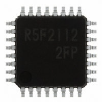
R5F21122FP#U0
Manufacturer Part Number
R5F21122FP#U0
Description
IC R8C MCU FLASH 8K 32LQFP
Manufacturer
Renesas Electronics America
Series
M16C™ M16C/R8C/Tiny/12r
Datasheets
1.R5F211A2SPU0.pdf
(300 pages)
2.R5F21122FPU0.pdf
(30 pages)
3.R5F21122FPU0.pdf
(200 pages)
Specifications of R5F21122FP#U0
Core Processor
R8C
Core Size
16-Bit
Speed
16MHz
Connectivity
SIO, UART/USART
Peripherals
LED, WDT
Number Of I /o
22
Program Memory Size
8KB (8K x 8)
Program Memory Type
FLASH
Ram Size
512 x 8
Voltage - Supply (vcc/vdd)
2.7 V ~ 5.5 V
Data Converters
A/D 8x10b
Oscillator Type
Internal
Operating Temperature
-20°C ~ 85°C
Package / Case
32-LQFP
For Use With
R0K521134S000BE - KIT EVAL STARTER FOR R8C/13R0E521134EPB00 - KIT EMULATOR PROBE FOR PC7501R0E521134CPE00 - EMULATOR COMPACT R8C/13
Lead Free Status / RoHS Status
Lead free / RoHS Compliant
Eeprom Size
-
Available stocks
Company
Part Number
Manufacturer
Quantity
Price


R8C/12 Group
Rev.1.20
REJ09B0110-0120
Figure 13.4 U0MR and U1MR Registers and U0C0 and U1C0 Registers
UARTi transmit/receive control register 0 (i=0, 1)
UARTi transmit/receive mode register (i=0, 1)
b 7
b 7
0
NOTES:
NOTES:
1. Must set the P1_6 bit in the PD1 register to “0” (input).
2. For the U1MR register, the SMD2 to SMD0 bits must not be set except the followings: “000
3. Must set the CKDIR bit to “0” (internal clock) in UART1.
1. If the BRG count source is switched, set the UiBRG register again.
b 6
b6
Jan 27, 2006
b 5
b 5
b 4
b 4
b 3
b 3
b 2
b 2
0
b 1
b 1
b 0
b 0
page 92 of 181
UFORM T r a n s f e r f o r m a t s e l e c t b i t
C K P O L
T X E P T
s y m b o l
CKDIR
symbol
S M D 0
S M D 1
S M D 2
PRYE
S T P S
CLK0
C L K 1
PRY
NCH
(b2)
( b 4 )
( b 7 )
B i t
Bit
S y m b o l
I n t e r n a l / e x t e r n a l c l o c k
s e l e c t b i t
S t o p b i t l e n g t h s e l e c t b i t
O d d / e v e n p a r i t y s e l e c t b i t
P a r i t y e n a b l e b i t
Reserved bit
Serial interface mode
select bit
S y m b o l
U 0 C 0
U 1 C 0
BRG count source
select bit
Transmit register empty
flag
Data output select bit
CLK polarity select bit
R e s e r v e d b i t
U 0 M R
U 1 M R
Nothing is assigned.
When write, set to “0”. When read, its content is indeterminate.
B i t n a m e
Bit name
(2)
(3 )
(1)
A d d r e s s
0 0 A C
0 0 A 4
A d d r e s s
0 0 A 0
0 0 A 8
0 0 : f
0 1 : f
1 0 : f
1 1 : Avoid this setting
0 : Data present in transmit register (during transmission)
1 : No data present in transmit register
0 : TxDi pin is a pin of CMOS output
1 : TxDi pin is a pin of N-channel open-drain output
0 : LSB first
1 : MSB first
0 : 1 s t o p b i t
1 : 2 s t o p b i t s
E f f e c t i v e w h e n P R Y E = 1
0 : O d d p a r i t y
1 : E v e n p a r i t y
0 : P a r i t y d i s a b l e d
1 : P a r i t y e n a b l e d
1 6
S e t t o “ 0 ”
0 : T r a n s m i t d a t a i s o u t p u t a t f a l l i n g e d g e o f t r a n s f e r c l o c k
1 : T r a n s m i t d a t a i s o u t p u t a t r i s i n g e d g e o f t r a n s f e r c l o c k
1 6
b 1 b 0
b2 b1 b0
0 0 0 : Serial interface disabled
0 0 1 : Clock synchronous serial I/O mode
1 0 0 : UART mode transfer data 7 bits long
1 0 1 : UART mode transfer data 8 bits long
1 1 0 : UART mode transfer data 9 bits long
Must not be set except above
0 : Internal clock
1 : External clock
Set to “0”
1 6
1 6
(transmission completed)
1SIO
8SIO
32SIO
a n d r e c e i v e d a t a i s i n p u t a t r i s i n g e d g e
a n d r e c e i v e d a t a i s i n p u t a t f a l l i n g e d g e
is selected
is selected
is selected
A f t e r r e s e t
A f t e r r e s e t
0 8
0 8
0 0
0 0
(1)
1 6
1 6
1 6
1 6
F u n c t i o n
F u n c t i o n
2
”, “100
2
”, “101
2
”, or “110
2
13. Serial Interface
”.
RW
R W
RW
R W
R W
R W
R W
R W
RW
RW
R W
R W
R W
R W
R W
R O
R W
Related parts for R5F21122FP#U0
Image
Part Number
Description
Manufacturer
Datasheet
Request
R

Part Number:
Description:
KIT STARTER FOR M16C/29
Manufacturer:
Renesas Electronics America
Datasheet:

Part Number:
Description:
KIT STARTER FOR R8C/2D
Manufacturer:
Renesas Electronics America
Datasheet:

Part Number:
Description:
R0K33062P STARTER KIT
Manufacturer:
Renesas Electronics America
Datasheet:

Part Number:
Description:
KIT STARTER FOR R8C/23 E8A
Manufacturer:
Renesas Electronics America
Datasheet:

Part Number:
Description:
KIT STARTER FOR R8C/25
Manufacturer:
Renesas Electronics America
Datasheet:

Part Number:
Description:
KIT STARTER H8S2456 SHARPE DSPLY
Manufacturer:
Renesas Electronics America
Datasheet:

Part Number:
Description:
KIT STARTER FOR R8C38C
Manufacturer:
Renesas Electronics America
Datasheet:

Part Number:
Description:
KIT STARTER FOR R8C35C
Manufacturer:
Renesas Electronics America
Datasheet:

Part Number:
Description:
KIT STARTER FOR R8CL3AC+LCD APPS
Manufacturer:
Renesas Electronics America
Datasheet:
Part Number:
Description:
KIT STARTER FOR RX610
Manufacturer:
Renesas Electronics America
Datasheet:

Part Number:
Description:
KIT STARTER FOR R32C/118
Manufacturer:
Renesas Electronics America
Datasheet:

Part Number:
Description:
KIT DEV RSK-R8C/26-29
Manufacturer:
Renesas Electronics America
Datasheet:

Part Number:
Description:
KIT STARTER FOR SH7124
Manufacturer:
Renesas Electronics America
Datasheet:

Part Number:
Description:
KIT STARTER FOR H8SX/1622
Manufacturer:
Renesas Electronics America
Datasheet:

Part Number:
Description:
KIT DEV FOR SH7203
Manufacturer:
Renesas Electronics America
Datasheet: