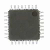
R5F21132FP#U0 Renesas Electronics America, R5F21132FP#U0 Datasheet - Page 146

R5F21132FP#U0
Manufacturer Part Number
R5F21132FP#U0
Description
IC R8C MCU FLASH 8K 32LQFP
Manufacturer
Renesas Electronics America
Series
M16C™ M16C/R8C/Tiny/13r
Datasheets
1.R5F211A2SPU0.pdf
(300 pages)
2.R5F21132FPU0.pdf
(33 pages)
3.R5F21132FPU0.pdf
(226 pages)
Specifications of R5F21132FP#U0
Core Processor
R8C
Core Size
16-Bit
Speed
20MHz
Connectivity
SIO, UART/USART
Peripherals
LED, POR, Voltage Detect, WDT
Number Of I /o
22
Program Memory Size
8KB (8K x 8)
Program Memory Type
FLASH
Ram Size
512 x 8
Voltage - Supply (vcc/vdd)
2.7 V ~ 5.5 V
Data Converters
A/D 12x10b
Oscillator Type
Internal
Operating Temperature
-20°C ~ 85°C
Package / Case
32-LQFP
For Use With
R0K521134S000BE - KIT EVAL STARTER FOR R8C/13R0E521134EPB00 - KIT EMULATOR PROBE FOR PC7501R0E521134CPE00 - EMULATOR COMPACT R8C/13
Lead Free Status / RoHS Status
Lead free / RoHS Compliant
Eeprom Size
-
Available stocks
Company
Part Number
Manufacturer
Quantity
Price
- Current page: 146 of 226
- Download datasheet (3Mb)
R8C/13 Group
Rev.1.20
REJ09B0111-0120
Figure 14.8 Internal Equivalent Circuit to Analog Input
14.5 Internal Equivalent Circuit of Analog Input
Figure 14.8 shows the internal equivalent circuit of analog input.
Parasitic
Parasitic
Jan 27, 2006
AN0
diode
diode
Warning: Use only as a standard for designing this data.
AV
V
Control signal
for SW2
Control signal
for SW3
REF
Comparison reference voltage (Vref) generator
SS
ANi
i =10
V
V
CC
SS
A/D control register 0
Mass production may cause some changes in device characteristics.
ON resistor
approx. 2k
ON resistor
approx. 2k
b2
V
page 133 of 205
CC
SW1
SW1
b1
i ladder-type
switches
(i = 10)
V
b0
SS
Sampling
Connect to
Connect to
Wiring resistor
approx. 0.2k
Wiring resistor
approx. 0.2k
Resistor
ladder
Comparison
Connect to
Connect to
i ladder-type
wiring resistors
(i = 10)
ON resistor
approx. 0.6k
Reference control
ON resistor
approx. 0.6k
SW2
control signal
SW2
Sampling
signal
Analog input voltage
V
SW1 conducts only on the ports selected for analog input.
SW2 and SW3 are open when A/D conversion is not in progress;
their status varies as shown by the waveforms in the diagrams on the left.
SW4 conducts only when A/D conversion is not in progress.
Vref
Comparison voltage
IN
14.5 Internal Equivalent Circuit of Analog Input
C = Approx.1.5pF
SW4
AV
AV
SS
A/D successive
conversion register
CC
ON resistor
approx. 5k
SW3
Chopper-type
amplifier
AMP
A/D conversion
interrupt request
Related parts for R5F21132FP#U0
Image
Part Number
Description
Manufacturer
Datasheet
Request
R

Part Number:
Description:
KIT STARTER FOR M16C/29
Manufacturer:
Renesas Electronics America
Datasheet:

Part Number:
Description:
KIT STARTER FOR R8C/2D
Manufacturer:
Renesas Electronics America
Datasheet:

Part Number:
Description:
R0K33062P STARTER KIT
Manufacturer:
Renesas Electronics America
Datasheet:

Part Number:
Description:
KIT STARTER FOR R8C/23 E8A
Manufacturer:
Renesas Electronics America
Datasheet:

Part Number:
Description:
KIT STARTER FOR R8C/25
Manufacturer:
Renesas Electronics America
Datasheet:

Part Number:
Description:
KIT STARTER H8S2456 SHARPE DSPLY
Manufacturer:
Renesas Electronics America
Datasheet:

Part Number:
Description:
KIT STARTER FOR R8C38C
Manufacturer:
Renesas Electronics America
Datasheet:

Part Number:
Description:
KIT STARTER FOR R8C35C
Manufacturer:
Renesas Electronics America
Datasheet:

Part Number:
Description:
KIT STARTER FOR R8CL3AC+LCD APPS
Manufacturer:
Renesas Electronics America
Datasheet:

Part Number:
Description:
KIT STARTER FOR RX610
Manufacturer:
Renesas Electronics America
Datasheet:

Part Number:
Description:
KIT STARTER FOR R32C/118
Manufacturer:
Renesas Electronics America
Datasheet:

Part Number:
Description:
KIT DEV RSK-R8C/26-29
Manufacturer:
Renesas Electronics America
Datasheet:

Part Number:
Description:
KIT STARTER FOR SH7124
Manufacturer:
Renesas Electronics America
Datasheet:

Part Number:
Description:
KIT STARTER FOR H8SX/1622
Manufacturer:
Renesas Electronics America
Datasheet:

Part Number:
Description:
KIT DEV FOR SH7203
Manufacturer:
Renesas Electronics America
Datasheet:


