R5F21132FP#U0 Renesas Electronics America, R5F21132FP#U0 Datasheet - Page 36
R5F21132FP#U0
Manufacturer Part Number
R5F21132FP#U0
Description
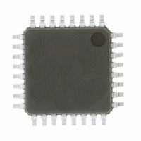
IC R8C MCU FLASH 8K 32LQFP
Manufacturer
Renesas Electronics America
Series
M16C™ M16C/R8C/Tiny/13r
Datasheets
1.R5F211A2SPU0.pdf
(300 pages)
2.R5F21132FPU0.pdf
(33 pages)
3.R5F21132FPU0.pdf
(226 pages)
Specifications of R5F21132FP#U0
Core Processor
R8C
Core Size
16-Bit
Speed
20MHz
Connectivity
SIO, UART/USART
Peripherals
LED, POR, Voltage Detect, WDT
Number Of I /o
22
Program Memory Size
8KB (8K x 8)
Program Memory Type
FLASH
Ram Size
512 x 8
Voltage - Supply (vcc/vdd)
2.7 V ~ 5.5 V
Data Converters
A/D 12x10b
Oscillator Type
Internal
Operating Temperature
-20°C ~ 85°C
Package / Case
32-LQFP
For Use With
R0K521134S000BE - KIT EVAL STARTER FOR R8C/13R0E521134EPB00 - KIT EMULATOR PROBE FOR PC7501R0E521134CPE00 - EMULATOR COMPACT R8C/13
Lead Free Status / RoHS Status
Lead free / RoHS Compliant
Eeprom Size
-
Available stocks
Company
Part Number
Manufacturer
Quantity
Price


R8C/13 Group
Rev.1.20
REJ09B0111-0120
Figure 5.9 D4INT Register
V o l t a g e d e t e c t i o n i n t e r r u p t r e g i s t e r
b 7
N O T E S :
1 0 . T h e s o f t w a r e r e s e t o r t h e w a t c h d o g t i m e r r e s e t d o n o t a f f e c t t h i s r e g i s t e r .
1 1 . W h e n t h e D 4 6 b i t i s s e t t o “ 1 ” ( h a r d w a r e r e s e t 2 w h e n V d e t p a s s e s ) , s e t t h e D 4 7 b i t t o “ 1 ” ( b e l o w V d e t ) .
1 . S e t t h e P R C 3 b i t i n t h e P R C R r e g i s t e r t o “ 1 ” ( w r i t e e n a b l e ) b e f o r e w r i t i n g t o t h i s r e g i s t e r .
2 . I f t h e v o l t a g e d e t e c t i o n i n t e r r u p t n e e d s t o b e u s e d t o g e t o u t o f s t o p m o d e a g a i n a f t e r o n c e u s e d f o r t h a t
3. V a l i d w h e n t h e V C 2 7 b i t i n t h e V C R 2 r e g i s t e r i s s e t t o “ 1 ” ( v o l t a g e d e t e c t i o n c i r c u i t e n a b l e d ) .
4 . I f t h e V C 2 7 b i t i s s e t t o “ 0 ” ( v o l t a g e d e t e c t i o n c i r c u i t d i s a b l e d ) , t h e D 4 2 a n d D 4 3 b i t s a r e s e t t o “ 0 ” ( n o t d e t e c t e d ) .
5 . T h i s b i t i s s e t t o “ 0 ” b y w r i t i n g a “ 0 ” i n a p r o g r a m . ( w r i t i n g a “ 1 ” h a s n o e f f e c t . )
6 . V a l i d w h e n t h e D 4 0 b i t i s s e t t o “ 1 ” ( v o l t a g e d e t e c t i o n i n t e r r u p t e n a b l e d ) .
7 . T h e D 4 0 b i t i s v a l i d w h e n t h e V C 2 7 b i t i n t h e V C R 2 r e g i s t e r i s s e t t o “ 1 ” ( v o l t a g e d e t e c t i o n c i r c u i t e n a b l e d ) .
8 . V a l i d w h e n t h e D 4 1 b i t i s s e t t o “ 1 ” ( d i g i t a l f i l t e r d i s a b l e d m o d e ) .
9 . T h e D 4 6 b i t c a n b e s e l e c t e d .
Jan 27, 2006
p u r p o s e , r e s e t t h e D 4 1 b i t b y w r i t i n g a “ 0 ” a n d t h e n a “ 1 ” .
W h e n s e t t i n g t h e D 4 0 b i t t o “ 1 ” , t h e f o l l o w i n g s e t t i n g i s r e q u i r e d .
( 1 ) S e t t h e V C 2 7 b i t “ 1 ” .
( 2 ) W a i t f o r t d ( E - A ) u n t i l t h e d e t e c t e r c i r c u i t o p e r a t e s .
( 3 ) W a i t f o r t h e s a m p l i n g t i m e ( t h e s a m p l i n g c l o c k w h i c h i s s e l e c t e d i n t h e D F 0 b i t t o D F 1 b i t t i m e s 4 c y c l e s . )
( 4 ) S e t t h e D 4 0 b i t t o “ 1 ” .
( 5 ) S e t t h e C M 1 4 b i t i n t h e C M 1 r e g i s t e r t o “ 0 ” ( l o w - s p e e d o n - c h i p o s c i l l a t o r o n ) .
b 6
( D o n o t s e t t o “ 0 ” ) .
b 5
b 4
b 3
b 2
page 23 of 205
b 1
b 0
Bit symbol
D 4 0
D 4 1
D 4 2
D 4 3
D F 0
DF1
D 4 6
D47
Symbol
D4INT
Voltage detection condition
select bit
Voltage detection interrupt
enable bit
Voltage detection digital filter
disable mode select bit
Voltage change detection
flag
WDT overflow detect flag
Sampling clock select bit
Voltage monitor mode select
bit
(1)
(6)
(3, 4, 5)
Address
001F
(11)
B i t n a m e
(7)
16
Reset input : 00
RESET pin = H retaining : 01000001
After reset
(3, 4)
b 5b 4
0 :
1 :
0 : D i g i t a l f i l t e r e n a b l e m o d e ( d i g i t a l
1 : D i g i t a l f i l t e r d i s a b l e m o d e ( d i g i t a l
0 : N o t d e t e c t e d
1 : V d e t p a s s i n g d e t e c t i o n
0: Not detected (flag clear)
1: Detected
00 : f
01 : f
10 : f
11 : f
0 : V o l t a g e d e t e c t i o n i n t e r r u p t
1 : H a r d w a r e r e s e t 2 w h e n
V o l t a g e d e t e c t i o n i n t e r r u p t
r e q u e s t i s g e n e r a t e d
o r h a r d w a r e r e s e t 2
w h e n V c c p a s s e s V d e t
0 : O v e r V d e t
1 : B e l o w V d e t
f i l t e r c i r c u i t e n a b l e d )
f i l t e r c i r c u i t d i s a b l e d )
r e q u e s t i s g e n e r a t e d w h e n
p a s s i n g t h r o u g h V d e t
p a s s i n g t h r o u g h V d e t
D i s a b l e
E n a b l e
(10)
RING-S
RING-S
RING-S
RING-S
16
divided by 1
divided by 2
divided by 4
divided by 8
F u n c t i o n
5.4 Voltage Detection Circuit
( 9 )
2
R W
R W
R W
R W
R W
RW
RW
R W
R W
Related parts for R5F21132FP#U0
Image
Part Number
Description
Manufacturer
Datasheet
Request
R

Part Number:
Description:
KIT STARTER FOR M16C/29
Manufacturer:
Renesas Electronics America
Datasheet:

Part Number:
Description:
KIT STARTER FOR R8C/2D
Manufacturer:
Renesas Electronics America
Datasheet:

Part Number:
Description:
R0K33062P STARTER KIT
Manufacturer:
Renesas Electronics America
Datasheet:

Part Number:
Description:
KIT STARTER FOR R8C/23 E8A
Manufacturer:
Renesas Electronics America
Datasheet:

Part Number:
Description:
KIT STARTER FOR R8C/25
Manufacturer:
Renesas Electronics America
Datasheet:

Part Number:
Description:
KIT STARTER H8S2456 SHARPE DSPLY
Manufacturer:
Renesas Electronics America
Datasheet:

Part Number:
Description:
KIT STARTER FOR R8C38C
Manufacturer:
Renesas Electronics America
Datasheet:

Part Number:
Description:
KIT STARTER FOR R8C35C
Manufacturer:
Renesas Electronics America
Datasheet:

Part Number:
Description:
KIT STARTER FOR R8CL3AC+LCD APPS
Manufacturer:
Renesas Electronics America
Datasheet:
Part Number:
Description:
KIT STARTER FOR RX610
Manufacturer:
Renesas Electronics America
Datasheet:

Part Number:
Description:
KIT STARTER FOR R32C/118
Manufacturer:
Renesas Electronics America
Datasheet:

Part Number:
Description:
KIT DEV RSK-R8C/26-29
Manufacturer:
Renesas Electronics America
Datasheet:

Part Number:
Description:
KIT STARTER FOR SH7124
Manufacturer:
Renesas Electronics America
Datasheet:

Part Number:
Description:
KIT STARTER FOR H8SX/1622
Manufacturer:
Renesas Electronics America
Datasheet:

Part Number:
Description:
KIT DEV FOR SH7203
Manufacturer:
Renesas Electronics America
Datasheet: