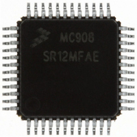
MC908SR12MFAE Freescale Semiconductor, MC908SR12MFAE Datasheet - Page 223

MC908SR12MFAE
Manufacturer Part Number
MC908SR12MFAE
Description
IC MCU 12K FLASH 8MHZ 48-LQFP
Manufacturer
Freescale Semiconductor
Series
HC08r
Datasheet
1.MC908SR12MFAE.pdf
(404 pages)
Specifications of MC908SR12MFAE
Core Processor
HC08
Core Size
8-Bit
Speed
8MHz
Connectivity
I²C, SCI
Peripherals
LVD, POR, PWM, Temp Sensor
Number Of I /o
31
Program Memory Size
12KB (12K x 8)
Program Memory Type
FLASH
Ram Size
512 x 8
Voltage - Supply (vcc/vdd)
4.5 V ~ 5.5 V
Data Converters
A/D 14x10b
Oscillator Type
Internal
Operating Temperature
-40°C ~ 125°C
Package / Case
48-LQFP
Lead Free Status / RoHS Status
Lead free / RoHS Compliant
Eeprom Size
-
Available stocks
Company
Part Number
Manufacturer
Quantity
Price
Company:
Part Number:
MC908SR12MFAE
Manufacturer:
Freescale Semiconductor
Quantity:
10 000
Company:
Part Number:
MC908SR12MFAER
Manufacturer:
Freescale Semiconductor
Quantity:
10 000
- Current page: 223 of 404
- Download datasheet (2Mb)
14.4 Functional Description
14.4.1 On-Chip Temperature Sensor
MC68HC908SR12•MC68HC08SR12 — Rev. 5.0
Freescale Semiconductor
Addr.
$000E
$000F
$0010
Analog Module Status and
Analog Module Control
Register Name
Analog Module Gain
Control Register
Control Register
(AMGCR)
(AMSCR)
Register
(AMCR)
Figure 14-2. Analog Module I/O Register Summary
Figure 14-1
component of the analog module is the two-stage gain amplifier used for
amplifying the small signals on the analog input pins, OPIN1 and OPIN2.
These two signals feed into a multiplexer together with the signal from
the internal temperature sensor and a reference input. The selected
signal is then fed into the two-stage gain amplifier before going into the
analog-to-digital converter (ADC) as OPOUT. The OPIN1 and OPIN2
pins can also feed directly into the ADC as channels ATD0 and ATD1
respectively, without any amplification.
The on-chip temperature sensor is designed to measure temperatures
from –20°C to 70 °C. The output of the internal temperature sensor
TSOUT is amplified by the two-stage amplifier. The amplified
temperature sensor signal is routed to the analog-to-digital converter for
analog-to-digital conversion (see
Reset:
Reset:
Reset:
Read:
Read:
Read:
Write:
Write:
Write:
AMCDIV1 AMCDIV0
GAINB3
PWR1
Bit 7
0
0
0
shows the block diagram of the analog module. The central
= Unimplemented
GAINB2
PWR0
Analog Module
6
0
0
0
GAINB1
OPCH1
OPIFR
U
5
0
0
0
U = Unaffected
GAINB0
OPCH0
OPIF
Figure
4
0
0
0
GAINA3
AMIEN
14-1).
3
0
0
0
0
GAINA2
DO2
DOF
2
0
0
0
Functional Description
GAINA1
CDIFR
DO1
U
0
Analog Module
1
0
0
Data Sheet
GAINA0
CDIF
Bit 0
DO0
0
0
0
223
Related parts for MC908SR12MFAE
Image
Part Number
Description
Manufacturer
Datasheet
Request
R
Part Number:
Description:
Manufacturer:
Freescale Semiconductor, Inc
Datasheet:
Part Number:
Description:
Manufacturer:
Freescale Semiconductor, Inc
Datasheet:
Part Number:
Description:
Manufacturer:
Freescale Semiconductor, Inc
Datasheet:
Part Number:
Description:
Manufacturer:
Freescale Semiconductor, Inc
Datasheet:
Part Number:
Description:
Manufacturer:
Freescale Semiconductor, Inc
Datasheet:
Part Number:
Description:
Manufacturer:
Freescale Semiconductor, Inc
Datasheet:
Part Number:
Description:
Manufacturer:
Freescale Semiconductor, Inc
Datasheet:
Part Number:
Description:
Manufacturer:
Freescale Semiconductor, Inc
Datasheet:
Part Number:
Description:
Manufacturer:
Freescale Semiconductor, Inc
Datasheet:
Part Number:
Description:
Manufacturer:
Freescale Semiconductor, Inc
Datasheet:
Part Number:
Description:
Manufacturer:
Freescale Semiconductor, Inc
Datasheet:
Part Number:
Description:
Manufacturer:
Freescale Semiconductor, Inc
Datasheet:
Part Number:
Description:
Manufacturer:
Freescale Semiconductor, Inc
Datasheet:
Part Number:
Description:
Manufacturer:
Freescale Semiconductor, Inc
Datasheet:
Part Number:
Description:
Manufacturer:
Freescale Semiconductor, Inc
Datasheet:


