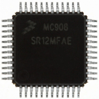
MC908SR12MFAE Freescale Semiconductor, MC908SR12MFAE Datasheet - Page 321

MC908SR12MFAE
Manufacturer Part Number
MC908SR12MFAE
Description
IC MCU 12K FLASH 8MHZ 48-LQFP
Manufacturer
Freescale Semiconductor
Series
HC08r
Datasheet
1.MC908SR12MFAE.pdf
(404 pages)
Specifications of MC908SR12MFAE
Core Processor
HC08
Core Size
8-Bit
Speed
8MHz
Connectivity
I²C, SCI
Peripherals
LVD, POR, PWM, Temp Sensor
Number Of I /o
31
Program Memory Size
12KB (12K x 8)
Program Memory Type
FLASH
Ram Size
512 x 8
Voltage - Supply (vcc/vdd)
4.5 V ~ 5.5 V
Data Converters
A/D 14x10b
Oscillator Type
Internal
Operating Temperature
-40°C ~ 125°C
Package / Case
48-LQFP
Lead Free Status / RoHS Status
Lead free / RoHS Compliant
Eeprom Size
-
Available stocks
Company
Part Number
Manufacturer
Quantity
Price
Company:
Part Number:
MC908SR12MFAE
Manufacturer:
Freescale Semiconductor
Quantity:
10 000
Company:
Part Number:
MC908SR12MFAER
Manufacturer:
Freescale Semiconductor
Quantity:
10 000
- Current page: 321 of 404
- Download datasheet (2Mb)
18.3.2 Data Direction Register A (DDRA)
MC68HC908SR12•MC68HC08SR12 — Rev. 5.0
Freescale Semiconductor
NOTE:
Address:
T1CH[1:0] — Timer 1 Channel I/O Bits
Care must be taken when reading port A while applying analog voltages
to ATD[7:2] pins. If the appropriate ADC channel is not enabled,
excessive current drain may occur if analog voltages are applied to the
PTAx/ATDx pin, while PTA is read as a digital input. Those ports not
selected as analog input channels are considered digital I/O ports.
LED drive — Direct LED drive Pins
Data direction register A determines whether each port A pin is an input
or an output. Writing a logic 1 to a DDRA bit enables the output buffer for
the corresponding port A pin; a logic 0 disables the output buffer.
DDRA[7:0] — Data Direction Register A Bits
Reset:
Read:
Write:
The T1CH1 and T1CH0 pins are the TIM1 input capture/output
compare pins. The edge/level select bits, ELSxB:ELSxA, determine
whether the PTA7/T1CH1 and PTA6/T1CH0 pins are timer channel
I/O pins or general-purpose I/O pins. See
Interface Module
PTA5–PTA0 pins can be configured for direct LED drive. See
Port A LED Control Register
These read/write bits control port A data direction. Reset clears
DDRA[7:0], configuring all port A pins as inputs.
1 = Corresponding port A pin configured as output
0 = Corresponding port A pin configured as input
DDRA7
$0004
Bit 7
0
Figure 18-3. Data Direction Register A (DDRA)
Input/Output (I/O) Ports
DDRA6
6
0
(TIM).
DDRA5
5
0
DDRA4
(LEDA).
4
0
DDRA3
3
0
Section 11. Timer
DDRA2
2
0
Input/Output (I/O) Ports
DDRA1
1
0
Data Sheet
18.3.3
DDRA0
Bit 0
Port A
0
321
Related parts for MC908SR12MFAE
Image
Part Number
Description
Manufacturer
Datasheet
Request
R
Part Number:
Description:
Manufacturer:
Freescale Semiconductor, Inc
Datasheet:
Part Number:
Description:
Manufacturer:
Freescale Semiconductor, Inc
Datasheet:
Part Number:
Description:
Manufacturer:
Freescale Semiconductor, Inc
Datasheet:
Part Number:
Description:
Manufacturer:
Freescale Semiconductor, Inc
Datasheet:
Part Number:
Description:
Manufacturer:
Freescale Semiconductor, Inc
Datasheet:
Part Number:
Description:
Manufacturer:
Freescale Semiconductor, Inc
Datasheet:
Part Number:
Description:
Manufacturer:
Freescale Semiconductor, Inc
Datasheet:
Part Number:
Description:
Manufacturer:
Freescale Semiconductor, Inc
Datasheet:
Part Number:
Description:
Manufacturer:
Freescale Semiconductor, Inc
Datasheet:
Part Number:
Description:
Manufacturer:
Freescale Semiconductor, Inc
Datasheet:
Part Number:
Description:
Manufacturer:
Freescale Semiconductor, Inc
Datasheet:
Part Number:
Description:
Manufacturer:
Freescale Semiconductor, Inc
Datasheet:
Part Number:
Description:
Manufacturer:
Freescale Semiconductor, Inc
Datasheet:
Part Number:
Description:
Manufacturer:
Freescale Semiconductor, Inc
Datasheet:
Part Number:
Description:
Manufacturer:
Freescale Semiconductor, Inc
Datasheet:


