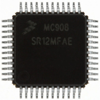
MC908SR12MFAE Freescale Semiconductor, MC908SR12MFAE Datasheet - Page 400

MC908SR12MFAE
Manufacturer Part Number
MC908SR12MFAE
Description
IC MCU 12K FLASH 8MHZ 48-LQFP
Manufacturer
Freescale Semiconductor
Series
HC08r
Datasheet
1.MC908SR12MFAE.pdf
(404 pages)
Specifications of MC908SR12MFAE
Core Processor
HC08
Core Size
8-Bit
Speed
8MHz
Connectivity
I²C, SCI
Peripherals
LVD, POR, PWM, Temp Sensor
Number Of I /o
31
Program Memory Size
12KB (12K x 8)
Program Memory Type
FLASH
Ram Size
512 x 8
Voltage - Supply (vcc/vdd)
4.5 V ~ 5.5 V
Data Converters
A/D 14x10b
Oscillator Type
Internal
Operating Temperature
-40°C ~ 125°C
Package / Case
48-LQFP
Lead Free Status / RoHS Status
Lead free / RoHS Compliant
Eeprom Size
-
Available stocks
Company
Part Number
Manufacturer
Quantity
Price
Company:
Part Number:
MC908SR12MFAE
Manufacturer:
Freescale Semiconductor
Quantity:
10 000
Company:
Part Number:
MC908SR12MFAER
Manufacturer:
Freescale Semiconductor
Quantity:
10 000
- Current page: 400 of 404
- Download datasheet (2Mb)
MC68HC08SR12
Data Sheet
400
Notes:
V
Run
Wait
Stop
Digital I/O ports Hi-Z leakage current
Input current
Capacitance
Ports (as input or output)
POR re-arm voltage
POR rise-time ramp rate
Monitor mode entry voltage
Pullup resistors
PTD[0:7] configured as KBI[0:7]
RST, IRQ1, IRQ2
Low-voltage inhibit, trip voltage
(No hysteresis implemented for 3V LVI)
Schmitt trigger input low level trip voltage
RST, IRQ1, IRQ2, KBI[0:7]
Schmitt trigger input high level trip voltage
RST, IRQ1, IRQ2, KBI[0:7]
1. V
2. Typical values reflect average measurements at midpoint of voltage range, 25 °C only.
3. Run (operating) I
4. Wait I
5. STOP I
6. Maximum is highest voltage that POR is guaranteed.
7. If minimum V
8. R
with ADC on
with ADC off
25°C (with OSC, TBM, LVI)
25°C (with OSC, TBM)
25°C
–40°C to 85°C (with OSC, TBM, LVI)
–40°C to 85°C (with OSC, TBM)
–40°C to 85°C
DD
100 pF on all outputs. C
Measured with all modules enabled.
all outputs. C
V
DD
PU1
(3)
DD
(4)
supply current
(5)
, f
, f
= 2.7 to 3.3 Vdc, V
is reached.
and R
DD
OP
OP
DD
measured using external square wave clock source. All inputs 0.2 V from rail. No dc loads. Less than 100 pF on
= 4.0 MHz
= 4.0 MHz
measured with OSC1 grounded, no port pins sourcing current.
PU2
DD
L
(8)
= 20 pF on OSC2. All ports configured as inputs. OSC2 capacitance linearly affects wait I
are measured at V
is not reached before the internal POR reset is released,
DD
Characteristic
(6)
measured using external square wave clock source. All inputs 0.2 V from rail. No dc loads. Less than
SS
(7)
L
= 0 Vdc, T
= 20 pF on OSC2. All ports configured as inputs. OSC2 capacitance linearly affects run I
Table A-3. 3V DC Electrical Characteristics
(1)
DD
A
= 5.0V.
= T
L
to T
H
, unless otherwise noted.
MC68HC08SR12
Symbol
V
V
C
V
R
R
R
V
SCMTH
SCMTL
C
V
I
I
I
OUT
POR
POR
DD
PU1
PU2
LVI3
IN
IL
IN
HI
MC68HC908SR12•MC68HC08SR12 — Rev. 5.0
RST
1.4 × V
0.035
Min
2.32
24
24
must be driven low externally until minimum
—
—
—
—
—
—
—
—
—
—
—
—
—
—
—
0
DD
Typ
2.49
2.5
1.5
0.8
1.2
27
35
35
—
—
—
—
—
—
—
—
—
—
7
5
5
(2)
Freescale Semiconductor
2.0 × V
Max
± 10
100
100
2.68
± 1
DD
16
12
80
12
15
12
42
42
—
—
—
6
5
5
8
.
DD
V/ms
Unit
mA
mA
mA
mV
µA
µA
µA
µA
µA
µA
µA
µA
kΩ
kΩ
pF
V
V
V
V
DD
.
Related parts for MC908SR12MFAE
Image
Part Number
Description
Manufacturer
Datasheet
Request
R
Part Number:
Description:
Manufacturer:
Freescale Semiconductor, Inc
Datasheet:
Part Number:
Description:
Manufacturer:
Freescale Semiconductor, Inc
Datasheet:
Part Number:
Description:
Manufacturer:
Freescale Semiconductor, Inc
Datasheet:
Part Number:
Description:
Manufacturer:
Freescale Semiconductor, Inc
Datasheet:
Part Number:
Description:
Manufacturer:
Freescale Semiconductor, Inc
Datasheet:
Part Number:
Description:
Manufacturer:
Freescale Semiconductor, Inc
Datasheet:
Part Number:
Description:
Manufacturer:
Freescale Semiconductor, Inc
Datasheet:
Part Number:
Description:
Manufacturer:
Freescale Semiconductor, Inc
Datasheet:
Part Number:
Description:
Manufacturer:
Freescale Semiconductor, Inc
Datasheet:
Part Number:
Description:
Manufacturer:
Freescale Semiconductor, Inc
Datasheet:
Part Number:
Description:
Manufacturer:
Freescale Semiconductor, Inc
Datasheet:
Part Number:
Description:
Manufacturer:
Freescale Semiconductor, Inc
Datasheet:
Part Number:
Description:
Manufacturer:
Freescale Semiconductor, Inc
Datasheet:
Part Number:
Description:
Manufacturer:
Freescale Semiconductor, Inc
Datasheet:
Part Number:
Description:
Manufacturer:
Freescale Semiconductor, Inc
Datasheet:


