MC908AZ60ACFUE Freescale Semiconductor, MC908AZ60ACFUE Datasheet - Page 168
MC908AZ60ACFUE
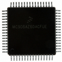
Manufacturer Part Number
MC908AZ60ACFUE
Description
IC MCU FLASH 8.4MHZ 60K 64QFP
Manufacturer
Freescale Semiconductor
Series
HC08r
Datasheet
1.MC908AZ60ACFUER.pdf
(414 pages)
Specifications of MC908AZ60ACFUE
Core Processor
HC08
Core Size
8-Bit
Speed
8.4MHz
Connectivity
CAN, SCI, SPI
Peripherals
LVD, POR, PWM
Number Of I /o
52
Program Memory Size
60KB (60K x 8)
Program Memory Type
FLASH
Eeprom Size
1K x 8
Ram Size
2K x 8
Voltage - Supply (vcc/vdd)
4.5 V ~ 5.5 V
Data Converters
A/D 15x8b
Oscillator Type
Internal
Operating Temperature
-40°C ~ 85°C
Package / Case
64-QFP
Lead Free Status / RoHS Status
Lead free / RoHS Compliant
Available stocks
Company
Part Number
Manufacturer
Quantity
Price
Company:

Part Number:
MC908AZ60ACFUE
Manufacturer:
Freescale Semiconductor
Quantity:
10 000
Part Number:
MC908AZ60ACFUE
Manufacturer:
FREESCALE
Quantity:
20 000
Company:
Part Number:
MC908AZ60ACFUE1L87J
Manufacturer:
TEMIC
Quantity:
350
Company:
Part Number:
MC908AZ60ACFUER
Manufacturer:
FREESCALE
Quantity:
5 560
Company:
Part Number:
MC908AZ60ACFUER
Manufacturer:
Freescale Semiconductor
Quantity:
10 000


Low-Voltage Inhibit (LVI)
16.3.1 Polled LVI Operation
In applications that can operate at V
polling the LVIOUT bit. In the configuration register, the LVIPWR bit must be at logic 1 to enable the LVI
module, and the LVIRST bit must be at logic 0 to disable LVI resets.
16.3.2 Forced Reset Operation
In applications that require V
module to reset the MCU when V
or more consecutive CPU cycles. In the configuration register, the LVIPWR and LVIRST bits must be at
logic 1 to enable the LVI module and to enable LVI resets.
16.3.3 False Reset Protection
The V
module to reset the MCU,V
CPU cycles. V
168
$FE0F
Addr.
DD
pin level is digitally filtered to reduce false resets due to power supply noise. In order for the LVI
DETECTOR
LVI Status Register (LVISR)
LOW V
DD
Register Name
V
DD
MC68HC908AZ60A • MC68HC908AS60A • MC68HC908AS60E Data Sheet, Rev. 6
must be above LVI
DD
V
V
DD
DD
> LVI
< LVI
DD
DD
TRIP
CPU CLOCK
TRIP
must remain at or below the LVI
Figure 16-1. LVI Module Block Diagram
Figure 16-2. LVI I/O Register Summary
= 0
= 1
to remain above the LVI
ANLGTRIP
FROM CONFIG-1
DD
Read: LVIOUT
Write:
LVIPWR
DD
falls to the LVI
TRIPR
levels below the LVI
Bit 7
DIGITAL FILTER
FROM CONFIG-1
Filter Bypass
Stop Mode
for only one CPU cycle to bring the MCU out of reset.
LVISTOP
V
DD
= Unimplemented
6
0
TRIPF
LVIOUT
TRIPF
level and remains at or below that level for nine
5
0
TRIPF
level, enabling LVI resets allows the LVI
TRIPF
FROM CONFIG-1
level, software can monitor V
LVIRST
4
0
level for nine or more consecutive
3
0
2
0
Freescale Semiconductor
LVI RESET
1
0
DD
by
Bit 0
0
Related parts for MC908AZ60ACFUE
Image
Part Number
Description
Manufacturer
Datasheet
Request
R

Part Number:
Description:
Manufacturer:
Freescale Semiconductor, Inc
Datasheet:
Part Number:
Description:
Manufacturer:
Freescale Semiconductor, Inc
Datasheet:
Part Number:
Description:
Manufacturer:
Freescale Semiconductor, Inc
Datasheet:
Part Number:
Description:
Manufacturer:
Freescale Semiconductor, Inc
Datasheet:
Part Number:
Description:
Manufacturer:
Freescale Semiconductor, Inc
Datasheet:
Part Number:
Description:
Manufacturer:
Freescale Semiconductor, Inc
Datasheet:
Part Number:
Description:
Manufacturer:
Freescale Semiconductor, Inc
Datasheet:
Part Number:
Description:
Manufacturer:
Freescale Semiconductor, Inc
Datasheet:
Part Number:
Description:
Manufacturer:
Freescale Semiconductor, Inc
Datasheet:
Part Number:
Description:
Manufacturer:
Freescale Semiconductor, Inc
Datasheet:
Part Number:
Description:
Manufacturer:
Freescale Semiconductor, Inc
Datasheet:
Part Number:
Description:
Manufacturer:
Freescale Semiconductor, Inc
Datasheet:
Part Number:
Description:
Manufacturer:
Freescale Semiconductor, Inc
Datasheet:
Part Number:
Description:
Manufacturer:
Freescale Semiconductor, Inc
Datasheet:
Part Number:
Description:
Manufacturer:
Freescale Semiconductor, Inc
Datasheet: