MC908AZ60ACFUE Freescale Semiconductor, MC908AZ60ACFUE Datasheet - Page 321
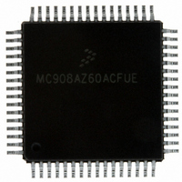
MC908AZ60ACFUE
Manufacturer Part Number
MC908AZ60ACFUE
Description
IC MCU FLASH 8.4MHZ 60K 64QFP
Manufacturer
Freescale Semiconductor
Series
HC08r
Datasheet
1.MC908AZ60ACFUER.pdf
(414 pages)
Specifications of MC908AZ60ACFUE
Core Processor
HC08
Core Size
8-Bit
Speed
8.4MHz
Connectivity
CAN, SCI, SPI
Peripherals
LVD, POR, PWM
Number Of I /o
52
Program Memory Size
60KB (60K x 8)
Program Memory Type
FLASH
Eeprom Size
1K x 8
Ram Size
2K x 8
Voltage - Supply (vcc/vdd)
4.5 V ~ 5.5 V
Data Converters
A/D 15x8b
Oscillator Type
Internal
Operating Temperature
-40°C ~ 85°C
Package / Case
64-QFP
Lead Free Status / RoHS Status
Lead free / RoHS Compliant
Available stocks
Company
Part Number
Manufacturer
Quantity
Price
Company:

Part Number:
MC908AZ60ACFUE
Manufacturer:
Freescale Semiconductor
Quantity:
10 000
Part Number:
MC908AZ60ACFUE
Manufacturer:
FREESCALE
Quantity:
20 000
Company:
Part Number:
MC908AZ60ACFUE1L87J
Manufacturer:
TEMIC
Quantity:
350
Company:
Part Number:
MC908AZ60ACFUER
Manufacturer:
FREESCALE
Quantity:
5 560
Company:
Part Number:
MC908AZ60ACFUER
Manufacturer:
Freescale Semiconductor
Quantity:
10 000


CHxF — Channel x Flag Bit
CHxIE — Channel x Interrupt Enable Bit
MSxB — Mode Select Bit B
MSxA — Mode Select Bit A
Freescale Semiconductor
When channel x is an input capture channel, this read/write bit is set when an active edge occurs on
the channel x pin. When channel x is an output compare channel, CHxF is set when the value in the
TIMA counter registers matches the value in the TIMA channel x registers.
When CHxIE = 1, clear CHxF by reading TIMA channel x status and control register with CHxF set and
then writing a logic 0 to CHxF. If another interrupt request occurs before the clearing sequence is
complete, then writing logic 0 to CHxF has no effect. Therefore, an interrupt request cannot be lost due
to inadvertent clearing of CHxF.
Reset clears the CHxF bit. Writing a logic 1 to CHxF has no effect.
This read/write bit enables TIMA CPU interrupts on channel x.
Reset clears the CHxIE bit.
This read/write bit selects buffered output compare/PWM operation. MSxB exists only in the TIMA
channel 0, TIMA channel 2 and TIMA channel 4 status and control registers.
Setting MS0B disables the channel 1 status and control register and reverts TACH1 pin to
general-purpose I/O.
Setting MS2B disables the channel 3 status and control register and reverts TACH3 pin to
general-purpose I/O.
Setting MS4B disables the channel 5 status and control register and reverts TACH5 pin to
general-purpose I/O.
Reset clears the MSxB bit.
When ELSxB:A ≠ 00, this read/write bit selects either input capture operation or unbuffered output
compare/PWM operation. See
1 = Input capture or output compare on channel x
0 = No input capture or output compare on channel x
1 = Channel x CPU interrupt requests enabled
0 = Channel x CPU interrupt requests disabled
1 = Buffered output compare/PWM operation enabled
0 = Buffered output compare/PWM operation disabled
1 = Unbuffered output compare/PWM operation
0 = Input capture operation
Figure 25-7. TIMA Channel Status and Control Registers (TASC0–TASC5) (Continued)
Register Name and Address
Reset:
Read:
Write:
MC68HC908AZ60A • MC68HC908AS60A • MC68HC908AS60E Data Sheet, Rev. 6
CH5F
Bit 7
R
0
0
= Reserved
CH5IE
6
0
Table
TASC5 — $0035
25-2.
5
0
R
0
MS5A
4
0
ELS5B
3
0
ELS5A
2
0
TOV5
1
0
CH5MAX
Bit 0
0
I/O Registers
321
Related parts for MC908AZ60ACFUE
Image
Part Number
Description
Manufacturer
Datasheet
Request
R

Part Number:
Description:
Manufacturer:
Freescale Semiconductor, Inc
Datasheet:
Part Number:
Description:
Manufacturer:
Freescale Semiconductor, Inc
Datasheet:
Part Number:
Description:
Manufacturer:
Freescale Semiconductor, Inc
Datasheet:
Part Number:
Description:
Manufacturer:
Freescale Semiconductor, Inc
Datasheet:
Part Number:
Description:
Manufacturer:
Freescale Semiconductor, Inc
Datasheet:
Part Number:
Description:
Manufacturer:
Freescale Semiconductor, Inc
Datasheet:
Part Number:
Description:
Manufacturer:
Freescale Semiconductor, Inc
Datasheet:
Part Number:
Description:
Manufacturer:
Freescale Semiconductor, Inc
Datasheet:
Part Number:
Description:
Manufacturer:
Freescale Semiconductor, Inc
Datasheet:
Part Number:
Description:
Manufacturer:
Freescale Semiconductor, Inc
Datasheet:
Part Number:
Description:
Manufacturer:
Freescale Semiconductor, Inc
Datasheet:
Part Number:
Description:
Manufacturer:
Freescale Semiconductor, Inc
Datasheet:
Part Number:
Description:
Manufacturer:
Freescale Semiconductor, Inc
Datasheet:
Part Number:
Description:
Manufacturer:
Freescale Semiconductor, Inc
Datasheet:
Part Number:
Description:
Manufacturer:
Freescale Semiconductor, Inc
Datasheet: