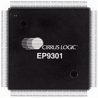
EP9301-CQZ Cirrus Logic Inc, EP9301-CQZ Datasheet - Page 490

EP9301-CQZ
Manufacturer Part Number
EP9301-CQZ
Description
IC ARM9 SOC PROCESSOR 208LQFP
Manufacturer
Cirrus Logic Inc
Series
EP9r
Specifications of EP9301-CQZ
Core Size
16/32-Bit
Peripherals
AC'97, DMA, I²:S, LED, MaverickKey, POR, PWM, WDT
Core Processor
ARM9
Speed
166MHz
Connectivity
EBI/EMI, Ethernet, I²C, IrDA, SPI, UART/USART, USB
Number Of I /o
19
Program Memory Type
ROMless
Ram Size
32K x 8
Voltage - Supply (vcc/vdd)
1.65 V ~ 3.6 V
Data Converters
A/D 5x12b
Oscillator Type
External
Operating Temperature
0°C ~ 70°C
Package / Case
208-TQFP, 208-VQFP
Controller Family/series
(ARM9)
No. Of I/o's
19
Ram Memory Size
16MB
Cpu Speed
166MHz
No. Of Timers
4
Digital Ic Case Style
TQFP
Embedded Interface Type
SPI
Rohs Compliant
Yes
Processor Series
EP93xx
Core
ARM920T
Data Bus Width
32 bit
3rd Party Development Tools
MDK-ARM, RL-ARM, ULINK2
Lead Free Status / RoHS Status
Lead free / RoHS Compliant
Eeprom Size
-
Program Memory Size
-
Lead Free Status / Rohs Status
Details
Other names
598-1136
Available stocks
Company
Part Number
Manufacturer
Quantity
Price
Company:
Part Number:
EP9301-CQZ
Manufacturer:
CIRRUS
Quantity:
3 390
Part Number:
EP9301-CQZ
Manufacturer:
CIRRUSLOGIC
Quantity:
20 000
Company:
Part Number:
EP9301-CQZR
Manufacturer:
Cirrus Logic Inc
Quantity:
10 000
- Current page: 490 of 824
- Download datasheet (13Mb)
12
12-12
Static Memory Controller
EP93xx User’s Guide
WPERR:
WP:
PME:
MW:
Copyright 2007 Cirrus Logic
The number of wait cycles for each of the 2nd, 3rd, and
4th accesses is specified by (WST2 + 1) HCLKs. For
example, if WST2 = 0x4, 4 + 1 = 5 cycles of HCLK are
inserted into the timing for each of the 2nd, 3rd, and 4th
accesses.
On reset, this field defaults to 0x1F (slowest access) to
enable booting from ROM or FLASH memory device
types.
Write Protect Error status flag - Read/Write
0 - No Error
1 - Write Protect Error
Writing a ‘1’ to this bit will clear the Write Protect status
error.
Write Protect - Read/Write
The value written to this bit specifies that either Writes to
the memory device are allowed to occur, or not occur:
0 - Yes (SRAM, FLASH)
1 - No (ROM, SRAM, FLASH)
Page Mode (Burst-of-4) Enable - Read/Write
0 - Page Mode is disabled, non-burst accesses occur
1 - Page Mode is enabled. Page Mode provides fast burst-
of-four accesses where the A[3] and A[4] address bits are
internally incremented, ‘00’ –> ‘01’ –> ‘10’ –> ‘11’, to
access four sequential words.
This bit is reset to ‘0’
Memory Width - Read/Write
The value written to this field specifies the bus-width of the
memory:
00 - 8-bit
01 - 16-bit
10 - 32-bit
11 - 32-bit
To support various bus-width memory devices for booting,
the MW field of the
automatically configured with the input values on the nCS7
and nCS6 pins, respectively. This takes place following a
power-on reset, but only if the input values on these pins
are: ASDO = ‘0’, Boot[1:0] = ‘00’, EEDAT = ‘1’. and EECLK
= ‘0’.
"SMCBCR[7:0]"
register can be
DS785UM1
Related parts for EP9301-CQZ
Image
Part Number
Description
Manufacturer
Datasheet
Request
R

Part Number:
Description:
32-Bit Microcontroller IC
Manufacturer:
Cirrus Logic Inc
Datasheet:

Part Number:
Description:
IC ARM920T MCU 166MHZ 208-LQFP
Manufacturer:
Cirrus Logic Inc
Datasheet:

Part Number:
Description:
IC ARM920T MCU 166MHZ 208-LQFP
Manufacturer:
Cirrus Logic Inc
Datasheet:

Part Number:
Description:
Development Kit
Manufacturer:
Cirrus Logic Inc
Datasheet:

Part Number:
Description:
Development Kit
Manufacturer:
Cirrus Logic Inc
Datasheet:

Part Number:
Description:
High-efficiency PFC + Fluorescent Lamp Driver Reference Design
Manufacturer:
Cirrus Logic Inc
Datasheet:

Part Number:
Description:
Development Kit
Manufacturer:
Cirrus Logic Inc
Datasheet:

Part Number:
Description:
Development Kit
Manufacturer:
Cirrus Logic Inc
Datasheet:

Part Number:
Description:
Development Kit
Manufacturer:
Cirrus Logic Inc
Datasheet:

Part Number:
Description:
Development Kit
Manufacturer:
Cirrus Logic Inc
Datasheet:

Part Number:
Description:
Development Kit
Manufacturer:
Cirrus Logic Inc
Datasheet:

Part Number:
Description:
Development Kit
Manufacturer:
Cirrus Logic Inc
Datasheet:

Part Number:
Description:
Ref Bd For Speakerbar MSA & DSP Products
Manufacturer:
Cirrus Logic Inc


