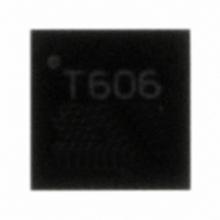
C8051T606-GM Silicon Laboratories Inc, C8051T606-GM Datasheet - Page 50

C8051T606-GM
Manufacturer Part Number
C8051T606-GM
Description
IC 8051 MCU 1.5K-EEPROM 11-QFN
Manufacturer
Silicon Laboratories Inc
Series
C8051T60xr
Specifications of C8051T606-GM
Program Memory Type
OTP
Program Memory Size
1.5KB (1.5K x 8)
Package / Case
11-QFN
Core Processor
8051
Core Size
8-Bit
Speed
25MHz
Connectivity
SMBus (2-Wire/I²C), UART/USART
Peripherals
POR, PWM, WDT
Number Of I /o
6
Ram Size
128 x 8
Voltage - Supply (vcc/vdd)
1.8 V ~ 3.6 V
Oscillator Type
Internal
Operating Temperature
-40°C ~ 85°C
Processor Series
C8051T6x
Core
8051
Data Bus Width
8 bit
Data Ram Size
128 B
Interface Type
I2C, UART
Maximum Clock Frequency
25 MHz
Number Of Programmable I/os
6
Number Of Timers
3
Operating Supply Voltage
1.8 V to 3.6 V
Maximum Operating Temperature
+ 85 C
Mounting Style
SMD/SMT
3rd Party Development Tools
PK51, CA51, A51, ULINK2
Development Tools By Supplier
C8051T606DK
Minimum Operating Temperature
- 40 C
Package
11QFN EP
Device Core
8051
Family Name
C8051T60x
Maximum Speed
25 MHz
Lead Free Status / RoHS Status
Lead free / RoHS Compliant
For Use With
336-1668 - CARD DAUGHTER QFN10 SOCKET336-1667 - CARD DAUGHTER MSOP SOCKET336-1666 - KIT DEVELOPMENT FOR C8051T606336-1404 - KIT DEV FOR C8051T60X MCU'S
Eeprom Size
-
Data Converters
-
Lead Free Status / Rohs Status
Lead free / RoHS Compliant
Other names
336-1662-5
Available stocks
Company
Part Number
Manufacturer
Quantity
Price
Company:
Part Number:
C8051T606-GM
Manufacturer:
SILICON
Quantity:
3 500
Part Number:
C8051T606-GM
Manufacturer:
SILICONLABS/èٹ¯ç§‘
Quantity:
20 000
C8051T600/1/2/3/4/5/6
9.5. ADC0 Analog Multiplexer (C8051T600/2/4 only)
ADC0 on the C8051T600/2/4 uses an analog input multiplexer to select the positive input to the ADC. Any
of the following may be selected as the positive input: Port 0 I/O pins, the on-chip temperature sensor, or
the positive power supply (V
SFR Definition 9.9.
Important Note About ADC0 Input Configuration: Port pins selected as ADC0 inputs should be config-
ured as analog inputs and should be skipped by the Digital Crossbar. To configure a Port pin for analog
input, set the corresponding bit in register PnMDIN to ‘0’. To force the Crossbar to skip a Port pin, set the
corresponding bit in register XBR0 to ‘1’. See Section “22. Port Input/Output” on page 106 for more Port
I/O configuration details.
50
Sensor
Temp
Figure 9.6. ADC0 Multiplexer Block Diagram
DD
). The ADC0 input channel is selected in the AMX0SL register described in
P0.0
P0.7
VDD
AMX0SL
Rev. 1.2
AMUX
ADC0


