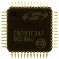
C8051F341-GQ Silicon Laboratories Inc, C8051F341-GQ Datasheet - Page 111

C8051F341-GQ
Manufacturer Part Number
C8051F341-GQ
Description
IC 8051 MCU FLASH 32K 48TQFP
Manufacturer
Silicon Laboratories Inc
Series
C8051F34xr
Datasheets
1.C8051F349-GQ.pdf
(276 pages)
2.C8051F341-GQ.pdf
(1 pages)
3.C8051F347-GQ.pdf
(296 pages)
Specifications of C8051F341-GQ
Program Memory Type
FLASH
Program Memory Size
32KB (32K x 8)
Package / Case
48-TQFP, 48-VQFP
Core Processor
8051
Core Size
8-Bit
Speed
48MHz
Connectivity
EBI/EMI, SMBus (2-Wire/I²C), SPI, UART/USART, USB
Peripherals
Brown-out Detect/Reset, POR, PWM, Temp Sensor, WDT
Number Of I /o
40
Ram Size
2.25K x 8
Voltage - Supply (vcc/vdd)
2.7 V ~ 3.6 V
Data Converters
A/D 20x10b
Oscillator Type
Internal
Operating Temperature
-40°C ~ 85°C
Processor Series
C8051F3x
Core
8051
Data Bus Width
8 bit
Data Ram Size
3.25 KB
Interface Type
I2C/SMBus/SPI/UART/USB
Maximum Clock Frequency
48 MHz
Number Of Programmable I/os
40
Number Of Timers
4
Operating Supply Voltage
2.7 V to 5.25 V
Maximum Operating Temperature
+ 85 C
Mounting Style
SMD/SMT
3rd Party Development Tools
KSK-SL-F34X, KSK-SL-TOOLSTICK, PK51, CA51, A51, ULINK2
Development Tools By Supplier
C8051F340DK
Minimum Operating Temperature
- 40 C
On-chip Adc
17-ch x 10-bit
No. Of I/o's
40
Ram Memory Size
2304Byte
Cpu Speed
48MHz
No. Of Timers
4
Rohs Compliant
Yes
Package
48TQFP
Device Core
8051
Family Name
C8051F34x
Maximum Speed
48 MHz
Data Rom Size
128 B
A/d Bit Size
10 bit
A/d Channels Available
17
Height
1 mm
Length
7 mm
Supply Voltage (max)
3.6 V
Supply Voltage (min)
2.7 V
Width
7 mm
Lead Free Status / RoHS Status
Lead free / RoHS Compliant
For Use With
336-1748 - ADAPTER TOOLSTICK FOR C8051F34X770-1006 - ISP 4PORT FOR SILABS C8051F MCU336-1452 - ADAPTER PROGRAM TOOLSTICK F340
Eeprom Size
-
Lead Free Status / Rohs Status
Lead free / RoHS Compliant
Other names
336-1299
Available stocks
Company
Part Number
Manufacturer
Quantity
Price
Company:
Part Number:
C8051F341-GQ
Manufacturer:
Silicon Laboratories Inc
Quantity:
10 000
Company:
Part Number:
C8051F341-GQR
Manufacturer:
Silicon Laboratories Inc
Quantity:
10 000
The level of FLASH security depends on the FLASH access method. The three FLASH access methods
that can be restricted are reads, writes, and erases from the C2 debug interface, user firmware executing
on unlocked pages, and user firmware executing on locked pages.
Accessing FLASH from the C2 debug interface:
Accessing FLASH from user firmware executing on an unlocked page:
Accessing FLASH from user firmware executing on a locked page:
1. Any unlocked page may be read, written, or erased.
2. Locked pages cannot be read, written, or erased.
3. The page containing the Lock Byte may be read, written, or erased if it is unlocked.
4. Reading the contents of the Lock Byte is always permitted.
5. Locking additional pages (changing ‘1’s to ‘0’s in the Lock Byte) is not permitted.
6. Unlocking FLASH pages (changing ‘0’s to ‘1’s in the Lock Byte) requires the C2 Device Erase
7. The Reserved Area cannot be read, written, or erased.
1. Any unlocked page except the page containing the Lock Byte may be read, written, or erased.
2. Locked pages cannot be read, written, or erased.
3. The page containing the Lock Byte cannot be erased. It may be read or written only if it is
4. Reading the contents of the Lock Byte is always permitted.
5. Locking additional pages (changing ‘1’s to ‘0’s in the Lock Byte) is not permitted.
6. Unlocking FLASH pages (changing ‘0’s to ‘1’s in the Lock Byte) is not permitted.
7. The Reserved Area cannot be read, written, or erased. Any attempt to access the reserved
1. Any unlocked page except the page containing the Lock Byte may be read, written, or erased.
2. Any locked page except the page containing the Lock Byte may be read, written, or erased.
3. The page containing the Lock Byte cannot be erased. It may only be read or written.
4. Reading the contents of the Lock Byte is always permitted.
5. Locking additional pages (changing ‘1’s to ‘0’s in the Lock Byte) is not permitted.
6. Unlocking FLASH pages (changing ‘0’s to ‘1’s in the Lock Byte) is not permitted.
7. The Reserved Area cannot be read, written, or erased. Any attempt to access the reserved
command, which erases all FLASH pages including the page containing the Lock Byte and the
Lock Byte itself.
unlocked.
area, or any other locked page, will result in a FLASH Error device reset.
area, or any other locked page, will result in a FLASH Error device reset.
C8051F340/1/2/3/4/5/6/7/8/9/A/B/C/D
Rev. 1.3
111


