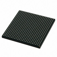
MCIMX512DJM8C Freescale Semiconductor, MCIMX512DJM8C Datasheet - Page 25

MCIMX512DJM8C
Manufacturer Part Number
MCIMX512DJM8C
Description
MULTIMEDIA PROC 529-LFBGA
Manufacturer
Freescale Semiconductor
Series
i.MX51r
Specifications of MCIMX512DJM8C
Core Processor
ARM Cortex-A8
Core Size
32-Bit
Speed
800MHz
Connectivity
1-Wire, EBI/EMI, Ethernet, I²C, IrDA, MMC, SPI, SSI, UART/USART, USB OTG
Peripherals
DMA, I²S, LCD, POR, PWM, WDT
Number Of I /o
128
Program Memory Type
ROMless
Ram Size
128K x 8
Voltage - Supply (vcc/vdd)
0.8 V ~ 1.15 V
Oscillator Type
External
Operating Temperature
-20°C ~ 85°C
Package / Case
529-LFBGA
Processor Series
i.MX51
Core
ARM Cortex A8
Data Bus Width
32 bit
Program Memory Size
36 KB
Data Ram Size
128 KB
Interface Type
I2C, SPI, SSI, UART, USB
Maximum Clock Frequency
200 MHz
Number Of Timers
5
Operating Supply Voltage
0.8 V to 1.15 V
Maximum Operating Temperature
+ 85 C
Mounting Style
SMD/SMT
3rd Party Development Tools
MDK-ARM, RL-ARM, ULINK2
Development Tools By Supplier
MCIMX51EVKJ
Minimum Operating Temperature
- 20 C
Lead Free Status / RoHS Status
Lead free / RoHS Compliant
Eeprom Size
-
Program Memory Size
-
Data Converters
-
Lead Free Status / Rohs Status
Lead free / RoHS Compliant
Available stocks
Company
Part Number
Manufacturer
Quantity
Price
Company:
Part Number:
MCIMX512DJM8C
Manufacturer:
Freescale Semiconductor
Quantity:
10 000
Part Number:
MCIMX512DJM8C
Manufacturer:
FREESCALE
Quantity:
20 000
4.3.1
The parameters in
1
2
3
Freescale Semiconductor
High-level output voltage
Low-level output voltage
Low-Level DC input voltage
Input Hysteresis
Schmitt trigger VT+
Schmitt trigger VT-
Input current (no pull-up/down)
Input current (22 kΩ Pull-up)
Input current (47 kΩ Pull-up)
Input current (100 kΩ Pull-up)
Input current (100 kΩ Pull-down)
Keeper Circuit Resistance
High-level output current
Low-level output current
High-Level DC input voltage
To maintain a valid level, the transition edge of the input must sustain a constant slew rate (monotonic) from the current DC
level through to the target DC level, VIL or VIH. Monotonic input transition time is from 0.1 ns to 1 s.
Hysteresis of 250 mV is guaranteed over all operating conditions when hysteresis is enabled.
I/O leakage currents are listed in
Parameter
GPIO/HSGPIO DC Parameters
The term OVDD in this section refers to the associated supply rail of an
input or output. The association is shown in
1, 2
1,
i.MX51 Applications Processors for Consumer and Industrial Products, Rev. 4
2
Table 18
1
1
Table 18. GPIO/HSGPIO DC Electrical Characteristics
are guaranteed per the operating ranges in
Table
Symbol
VHYS
VT+
Voh
VIH
VIL
VT-
Vol
Ioh
Iol
Iin
Iin
Iin
Iin
Iin
—
25.
Vout = 0.8
Vout = 0.2
Low drive
Medium drive
High drive
Max drive
Low drive
Medium drive
High drive
Max drive
Test Conditions
Vin = OVDD or 0
OVDD = 1.875V
OVDD = 2.775V
OVDD = 1.875
OVDD = 2.775
Iout = -1 mA
Vin = OVDD
Iout = 1mA
Vin = 0
Vin = 0
Vin = 0
NOTE
×
×
—
—
—
—
OVDD
OVDD
Table 128
OVDD –0.15
0.7
0.5OVDD
×
–1.9
–3.7
–5.2
–6.6
0.25
Min
1.9
3.7
5.2
6.6
—
—
—
—
—
—
—
—
—
0
and
OVDD
Table
Table
13, unless otherwise noted.
0.34
0.45
Typ
—
—
—
—
—
—
—
—
—
—
—
—
—
22
17
131.
Electrical Characteristics
0.5
OVDD + 0.3
0.3
See Note
OVDD
×
×
Max
0.15
161
76
36
36
—
—
—
—
—
—
OVDD
OVDD
3
Unit
mA
mA
μA
μA
μA
μA
kΩ
—
V
V
V
V
V
V
V
25


