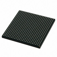
MCIMX512DJM8C Freescale Semiconductor, MCIMX512DJM8C Datasheet - Page 47

MCIMX512DJM8C
Manufacturer Part Number
MCIMX512DJM8C
Description
MULTIMEDIA PROC 529-LFBGA
Manufacturer
Freescale Semiconductor
Series
i.MX51r
Specifications of MCIMX512DJM8C
Core Processor
ARM Cortex-A8
Core Size
32-Bit
Speed
800MHz
Connectivity
1-Wire, EBI/EMI, Ethernet, I²C, IrDA, MMC, SPI, SSI, UART/USART, USB OTG
Peripherals
DMA, I²S, LCD, POR, PWM, WDT
Number Of I /o
128
Program Memory Type
ROMless
Ram Size
128K x 8
Voltage - Supply (vcc/vdd)
0.8 V ~ 1.15 V
Oscillator Type
External
Operating Temperature
-20°C ~ 85°C
Package / Case
529-LFBGA
Processor Series
i.MX51
Core
ARM Cortex A8
Data Bus Width
32 bit
Program Memory Size
36 KB
Data Ram Size
128 KB
Interface Type
I2C, SPI, SSI, UART, USB
Maximum Clock Frequency
200 MHz
Number Of Timers
5
Operating Supply Voltage
0.8 V to 1.15 V
Maximum Operating Temperature
+ 85 C
Mounting Style
SMD/SMT
3rd Party Development Tools
MDK-ARM, RL-ARM, ULINK2
Development Tools By Supplier
MCIMX51EVKJ
Minimum Operating Temperature
- 20 C
Lead Free Status / RoHS Status
Lead free / RoHS Compliant
Eeprom Size
-
Program Memory Size
-
Data Converters
-
Lead Free Status / Rohs Status
Lead free / RoHS Compliant
Available stocks
Company
Part Number
Manufacturer
Quantity
Price
Company:
Part Number:
MCIMX512DJM8C
Manufacturer:
Freescale Semiconductor
Quantity:
10 000
Part Number:
MCIMX512DJM8C
Manufacturer:
FREESCALE
Quantity:
20 000
- Current page: 47 of 200
- Download datasheet (6Mb)
4.6.2
Figure 13
4.6.3
The AUDMUX provides a programmable interconnect logic for voice, audio and data routing between
internal serial interfaces (SSIs) and external serial interfaces (audio and voice codecs). The AC timing of
AUDMUX external pins is hence governed by the SSI module.
4.6.4
The input to Clock Amplifier (CAMP) is internally ac-coupled allowing direct interface to a square wave
or sinusoidal frequency source. No external series capacitors are required.
electrical parameters.
Freescale Semiconductor
Input frequency
VIL (for square wave input)
VIH (for square wave input)
Sinusoidal input amplitude
Output duty cycle
CC5
ID
shows the WDOG reset timing and
WDOG Reset Timing Parameters
AUDMUX Timing Parameters
Clock Amplifier Parameters (CKIH1, CKIH2)
WATCHDOG_RST
CKIL is approximately 32 kHz. T
Parameter
Duration of WATCHDOG_RESET Assertion
i.MX51 Applications Processors for Consumer and Industrial Products, Rev. 4
(Input)
Table 47. CAMP Electrical Parameters (CKIH1, CKIH2)
Table 46. WATCHDOG_RST Timing Parameters
Figure 13. WATCHDOG_RST Timing Diagram
Parameter
NVCC_PER3 - 0.25
Min
0.4
8.0
45
0
Table 46
CKIL
NOTE
is one period or approximately 30 μs.
lists the timing parameters.
CC5
Typ
—
—
—
—
50
Min
1
NVCC_PER3
Table 47
VDD
Max
40.0
0.3
55
Max
Electrical Characteristics
—
shows the CAMP
MHz
Vp-p
Unit
T
%
Unit
V
V
CKIL
47
Related parts for MCIMX512DJM8C
Image
Part Number
Description
Manufacturer
Datasheet
Request
R
Part Number:
Description:
MCIMX-LVDS1
Manufacturer:
Freescale Semiconductor
Datasheet:
Part Number:
Description:
Manufacturer:
Freescale Semiconductor, Inc
Datasheet:
Part Number:
Description:
Manufacturer:
Freescale Semiconductor, Inc
Datasheet:
Part Number:
Description:
Manufacturer:
Freescale Semiconductor, Inc
Datasheet:
Part Number:
Description:
Manufacturer:
Freescale Semiconductor, Inc
Datasheet:
Part Number:
Description:
Manufacturer:
Freescale Semiconductor, Inc
Datasheet:
Part Number:
Description:
Manufacturer:
Freescale Semiconductor, Inc
Datasheet:
Part Number:
Description:
Manufacturer:
Freescale Semiconductor, Inc
Datasheet:
Part Number:
Description:
Manufacturer:
Freescale Semiconductor, Inc
Datasheet:
Part Number:
Description:
Manufacturer:
Freescale Semiconductor, Inc
Datasheet:
Part Number:
Description:
Manufacturer:
Freescale Semiconductor, Inc
Datasheet:
Part Number:
Description:
Manufacturer:
Freescale Semiconductor, Inc
Datasheet:
Part Number:
Description:
Manufacturer:
Freescale Semiconductor, Inc
Datasheet:
Part Number:
Description:
Manufacturer:
Freescale Semiconductor, Inc
Datasheet:
Part Number:
Description:
Manufacturer:
Freescale Semiconductor, Inc
Datasheet:


