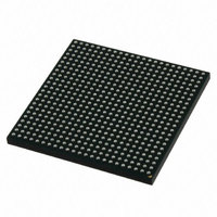
MCIMX512DJM8C Freescale Semiconductor, MCIMX512DJM8C Datasheet - Page 65

MCIMX512DJM8C
Manufacturer Part Number
MCIMX512DJM8C
Description
MULTIMEDIA PROC 529-LFBGA
Manufacturer
Freescale Semiconductor
Series
i.MX51r
Specifications of MCIMX512DJM8C
Core Processor
ARM Cortex-A8
Core Size
32-Bit
Speed
800MHz
Connectivity
1-Wire, EBI/EMI, Ethernet, I²C, IrDA, MMC, SPI, SSI, UART/USART, USB OTG
Peripherals
DMA, I²S, LCD, POR, PWM, WDT
Number Of I /o
128
Program Memory Type
ROMless
Ram Size
128K x 8
Voltage - Supply (vcc/vdd)
0.8 V ~ 1.15 V
Oscillator Type
External
Operating Temperature
-20°C ~ 85°C
Package / Case
529-LFBGA
Processor Series
i.MX51
Core
ARM Cortex A8
Data Bus Width
32 bit
Program Memory Size
36 KB
Data Ram Size
128 KB
Interface Type
I2C, SPI, SSI, UART, USB
Maximum Clock Frequency
200 MHz
Number Of Timers
5
Operating Supply Voltage
0.8 V to 1.15 V
Maximum Operating Temperature
+ 85 C
Mounting Style
SMD/SMT
3rd Party Development Tools
MDK-ARM, RL-ARM, ULINK2
Development Tools By Supplier
MCIMX51EVKJ
Minimum Operating Temperature
- 20 C
Lead Free Status / RoHS Status
Lead free / RoHS Compliant
Eeprom Size
-
Program Memory Size
-
Data Converters
-
Lead Free Status / Rohs Status
Lead free / RoHS Compliant
Available stocks
Company
Part Number
Manufacturer
Quantity
Price
Company:
Part Number:
MCIMX512DJM8C
Manufacturer:
Freescale Semiconductor
Quantity:
10 000
Part Number:
MCIMX512DJM8C
Manufacturer:
FREESCALE
Quantity:
20 000
- Current page: 65 of 200
- Download datasheet (6Mb)
Figure 33
timing parameters for this diagram is shown in
1
2
Freescale Semiconductor
DD24 DQS - DQ Skew (defines the Data valid window in read cycles
DD25 DQS DQ in HOLD time from DQS
DD26 DQS output access time from SDCLK posedge
ID
Test conditions are: Capacitance 15 pF for DDR PADS. Recommended drive strengths is medium for SDCLK and high for
address and controls
SDRAM CLK and DQS related parameters are being measured from the 50% point. that is, high is defined as 50% of signal
value and low is defined as 50% as signal value. DDR SDRAM CLK parameters are measured at the crossing point of SDCLK
and SDCLK (inverted clock)
DQS (input)
DQ (input)
SDCLK_B
related to DQS)
SDCLK
shows the timing diagram for mDDR SDRAM DQ versus DQS and SDCLK read cycle. The
Figure 33. mDDR SDRAM DQ vs. DQS and SDCLK READ Cycle Timing Diagram
i.MX51 Applications Processors for Consumer and Industrial Products, Rev. 4
DD26
Table 57. mDDR SDRAM Read Cycle Parameter Table
PARAMETER
DD24
Data
DD25
Data
Table
Data
57.
Data
Symbol
t
t
DQSCK
DQSQ
t
QH
Data
1.75
200 MHz
Min Max Min Max Min Max
—
2
0.4
—
5
Data
1
2
2.05
166 MHz
—
2
Electrical Characteristics
0.75
Data
5.5
—
2.6
133 MHz
—
2
Data
0.85
6.5
—
Unit
ns
ns
ns
65
Related parts for MCIMX512DJM8C
Image
Part Number
Description
Manufacturer
Datasheet
Request
R
Part Number:
Description:
MCIMX-LVDS1
Manufacturer:
Freescale Semiconductor
Datasheet:
Part Number:
Description:
Manufacturer:
Freescale Semiconductor, Inc
Datasheet:
Part Number:
Description:
Manufacturer:
Freescale Semiconductor, Inc
Datasheet:
Part Number:
Description:
Manufacturer:
Freescale Semiconductor, Inc
Datasheet:
Part Number:
Description:
Manufacturer:
Freescale Semiconductor, Inc
Datasheet:
Part Number:
Description:
Manufacturer:
Freescale Semiconductor, Inc
Datasheet:
Part Number:
Description:
Manufacturer:
Freescale Semiconductor, Inc
Datasheet:
Part Number:
Description:
Manufacturer:
Freescale Semiconductor, Inc
Datasheet:
Part Number:
Description:
Manufacturer:
Freescale Semiconductor, Inc
Datasheet:
Part Number:
Description:
Manufacturer:
Freescale Semiconductor, Inc
Datasheet:
Part Number:
Description:
Manufacturer:
Freescale Semiconductor, Inc
Datasheet:
Part Number:
Description:
Manufacturer:
Freescale Semiconductor, Inc
Datasheet:
Part Number:
Description:
Manufacturer:
Freescale Semiconductor, Inc
Datasheet:
Part Number:
Description:
Manufacturer:
Freescale Semiconductor, Inc
Datasheet:
Part Number:
Description:
Manufacturer:
Freescale Semiconductor, Inc
Datasheet:


