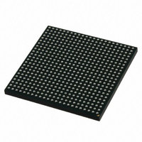
MCIMX515CJM6C Freescale Semiconductor, MCIMX515CJM6C Datasheet - Page 93

MCIMX515CJM6C
Manufacturer Part Number
MCIMX515CJM6C
Description
MULTIMEDIA PROC 529-LFBGA
Manufacturer
Freescale Semiconductor
Series
i.MX51r
Datasheets
1.MCIMX512DJM8C.pdf
(200 pages)
2.MCIMX515DJM8C.pdf
(2 pages)
3.MCIMX512CJM6C.pdf
(198 pages)
Specifications of MCIMX515CJM6C
Core Processor
ARM Cortex-A8
Core Size
32-Bit
Speed
600MHz
Connectivity
1-Wire, EBI/EMI, Ethernet, I²C, IrDA, MMC, SPI, SSI, UART/USART, USB OTG
Peripherals
DMA, I²S, LCD, POR, PWM, WDT
Number Of I /o
128
Program Memory Type
ROMless
Ram Size
128K x 8
Voltage - Supply (vcc/vdd)
0.8 V ~ 1.15 V
Oscillator Type
External
Operating Temperature
-20°C ~ 85°C
Package / Case
529-LFBGA
Processor Series
i.MX51
Core
ARM Cortex A8
Data Bus Width
32 bit
Program Memory Size
36 KB
Data Ram Size
128 KB
Interface Type
I2C, SPI, SSI, UART, USB
Maximum Clock Frequency
200 MHz
Number Of Timers
5
Operating Supply Voltage
0.8 V to 1.15 V
Maximum Operating Temperature
+ 95 C
Mounting Style
SMD/SMT
3rd Party Development Tools
MDK-ARM, RL-ARM, ULINK2
Development Tools By Supplier
MCIMX51EVKJ
Minimum Operating Temperature
- 40 C
Lead Free Status / RoHS Status
Lead free / RoHS Compliant
Eeprom Size
-
Program Memory Size
-
Data Converters
-
Lead Free Status / Rohs Status
Lead free / RoHS Compliant
Available stocks
Company
Part Number
Manufacturer
Quantity
Price
Company:
Part Number:
MCIMX515CJM6C
Manufacturer:
Freescale Semiconductor
Quantity:
10 000
Part Number:
MCIMX515CJM6C
Manufacturer:
FREESCALE
Quantity:
20 000
Company:
Part Number:
MCIMX515CJM6CR2
Manufacturer:
Freescale Semiconductor
Quantity:
10 000
The maximal accuracy of UP/DOWN edge of IPP_DATA is
The DISP_CLK_PERIOD, DI_CLK_PERIOD parameters are programmed via registers.
Figure 55
DISP_CLK_UP parameters are set via the Register.
Freescale Semiconductor
1
These conditions may be chip specific.
IP16
IP17
IP18
IP19
IP20o
IP20
The exact conditions have not been finalized, but will likely match the current customer requirement for their specific display.
ID
IPP_DISP_CLK
IPP_DATA
other controls
VSYNC
HSYNC
DRDY
Display interface clock
low time
Display interface clock
high time
Data setup time
Data holdup time
Control signals offset
times (defines for each
pin)
Control signals setup
time to display interface
clock (defines for each
pin)
depicts the synchronous display interface timing for access level. The DISP_CLK_DOWN and
Table 81. Synchronous Display Interface Timing Characteristics (Access Level)
Parameter
Figure 55. Synchronous Display Interface Timing Diagram—Access Level
i.MX51 Applications Processors for Consumer and Industrial Products, Rev. 4
IP16
Symbol
Tckl
Tckh
Tdsu
Tdhd
Tocsu
Tcsu
IP17
Tdicd-Tdicu–1.5
Tdicp–Tdicd+Tdicu–1.5
Tdicd–1.5
Tdicp–Tdicd–1.5
Tocsu–1.5
Tdicd–1.5–Tocsu%Tdicp Tdicu
Accuracy
IP19
local start point
Min
=
IP20o
T
diclk
IP18
Tdicu
IP20
±
0.75ns
Tdicd
Tdicp–Tdicd+Tdicu
Tdicu
Tdicp–Tdicu
Tocsu
Tdicd
2
–Tdicu
Typ
1
3
Tdicd–Tdicu+1.5
Tdicp–Tdicd+Tdicu+1.5
Tocsu+1.5
Electrical Characteristics
Max
—
—
—
Unit
ns
ns
ns
ns
ns
—
93


