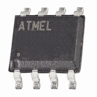
ATTINY25V-15ST Atmel, ATTINY25V-15ST Datasheet - Page 101

ATTINY25V-15ST
Manufacturer Part Number
ATTINY25V-15ST
Description
MCU AVR 2K FLASH 4MHZ 8-SOIC
Manufacturer
Atmel
Series
AVR® ATtinyr
Datasheet
1.ATTINY25-15MZ.pdf
(196 pages)
Specifications of ATTINY25V-15ST
Package / Case
8-SOIC (3.9mm Width)
Voltage - Supply (vcc/vdd)
1.8 V ~ 3.6 V
Operating Temperature
-40°C ~ 85°C
Speed
8MHz
Number Of I /o
6
Eeprom Size
128 x 8
Core Processor
AVR
Program Memory Type
FLASH
Ram Size
128 x 8
Program Memory Size
2KB (2K x 8)
Data Converters
A/D 4x10b
Oscillator Type
Internal
Peripherals
Brown-out Detect/Reset, POR, PWM, WDT
Connectivity
USI
Core Size
8-Bit
Processor Series
ATTINY2x
Core
AVR8
Data Bus Width
8 bit
Data Ram Size
128 B
Maximum Operating Temperature
+ 85 C
Mounting Style
SMD/SMT
Lead Free Status / RoHS Status
Lead free / RoHS Compliant
Available stocks
Company
Part Number
Manufacturer
Quantity
Price
Part Number:
ATTINY25V-15ST
Manufacturer:
ATMEL/爱特梅尔
Quantity:
20 000
- Current page: 101 of 196
- Download datasheet (4Mb)
7598H–AVR–07/09
Figure 16-4. Two-wire Mode Operation, Simplified Diagram
Figure 16-4
It is only the physical layer that is shown since the system operation is highly dependent of the
communication scheme used. The main differences between the Master and Slave operation at
this level, is the serial clock generation which is always done by the Master, and only the Slave
uses the clock control unit. Clock generation must be implemented in software, but the shift
operation is done automatically by both devices. Note that only clocking on negative edge for
shifting data is of practical use in this mode. The slave can insert wait states at start or end of
transfer by forcing the SCL clock low. This means that the Master must always check if the SCL
line was actually released after it has generated a positive edge.
Since the clock also increments the counter, a counter overflow can be used to indicate that the
transfer is completed. The clock is generated by the master by toggling the USCK pin via the
PORT Register.
The data direction is not given by the physical layer. A protocol, like the one used by the
TWI-bus, must be implemented to control the data flow.
Figure 16-5. Two-wire Mode, Typical Timing Diagram
SDA
SCL
SLAVE
MASTER
shows two USI units operating in Two-wire mode, one as Master and one as Slave.
Bit7
Bit7
S
A B
Bit6
Bit6
Bit5
Bit5
C
ADDRESS
1 - 7
Bit4
Bit4
Bit3
Bit3
R/W
8
Bit2
Bit2
D
Bit1
Bit1
ACK
9
Bit0
Bit0
E
DATA
1 - 8
Two-wire Clock
Control Unit
ACK
9
PORTxn
DATA
1 - 8
HOLD
ATtiny25/45/85
SCL
SDA
SCL
SDA
SCL
ACK
9
VCC
F
P
101
Related parts for ATTINY25V-15ST
Image
Part Number
Description
Manufacturer
Datasheet
Request
R

Part Number:
Description:
IC MCU AVR 2K FLASH 10MHZ 20-QFN
Manufacturer:
Atmel
Datasheet:

Part Number:
Description:
MCU AVR 2KB FLASH 10MHZ 8SOIC
Manufacturer:
Atmel
Datasheet:

Part Number:
Description:
IC AVR MCU 2K 10MHZ 8-DIP
Manufacturer:
Atmel
Datasheet:

Part Number:
Description:
IC MCU AVR 2KB FLASH 10MHZ 8SOIC
Manufacturer:
Atmel
Datasheet:

Part Number:
Description:
IC MCU AVR 2KB FLASH 10MHZ 8SOIC
Manufacturer:
Atmel
Datasheet:

Part Number:
Description:
MCU AVR 2KB FLASH 10MHZ 8SOIC
Manufacturer:
Atmel
Datasheet:

Part Number:
Description:
MCU AVR 2KB FLASH 10MHZ 20QFN
Manufacturer:
Atmel
Datasheet:

Part Number:
Description:
MCU AVR 2K ISP FLASH 1.8V 8-SOIC
Manufacturer:
Atmel
Datasheet:

Part Number:
Description:
IC AVR MCU 2K 10MHZ 8DIP
Manufacturer:
Atmel
Datasheet:

Part Number:
Description:
IC AVR MCU 2K 10MHZ 8SOIC
Manufacturer:
Atmel
Datasheet:

Part Number:
Description:
8-bit Microcontrollers - MCU 2KB FLASH,128B EE, 128B SRAM-10MHz
Manufacturer:
Atmel

Part Number:
Description:
8-bit Microcontrollers - MCU 2KB FL,128B EE,128B SRAM-10MHz
Manufacturer:
Atmel

Part Number:
Description:
8-bit Microcontrollers - MCU AVR 16KB FL 512B EE 1KB SRAM 10 MHZ GRN
Manufacturer:
Atmel


