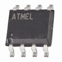
ATTINY25V-15ST Atmel, ATTINY25V-15ST Datasheet - Page 95

ATTINY25V-15ST
Manufacturer Part Number
ATTINY25V-15ST
Description
MCU AVR 2K FLASH 4MHZ 8-SOIC
Manufacturer
Atmel
Series
AVR® ATtinyr
Datasheet
1.ATTINY25-15MZ.pdf
(196 pages)
Specifications of ATTINY25V-15ST
Package / Case
8-SOIC (3.9mm Width)
Voltage - Supply (vcc/vdd)
1.8 V ~ 3.6 V
Operating Temperature
-40°C ~ 85°C
Speed
8MHz
Number Of I /o
6
Eeprom Size
128 x 8
Core Processor
AVR
Program Memory Type
FLASH
Ram Size
128 x 8
Program Memory Size
2KB (2K x 8)
Data Converters
A/D 4x10b
Oscillator Type
Internal
Peripherals
Brown-out Detect/Reset, POR, PWM, WDT
Connectivity
USI
Core Size
8-Bit
Processor Series
ATTINY2x
Core
AVR8
Data Bus Width
8 bit
Data Ram Size
128 B
Maximum Operating Temperature
+ 85 C
Mounting Style
SMD/SMT
Lead Free Status / RoHS Status
Lead free / RoHS Compliant
Available stocks
Company
Part Number
Manufacturer
Quantity
Price
Part Number:
ATTINY25V-15ST
Manufacturer:
ATMEL/爱特梅尔
Quantity:
20 000
- Current page: 95 of 196
- Download datasheet (4Mb)
15.2
15.3
7598H–AVR–07/09
Timer/Counter1 Dead Time A - DT1A
Timer/Counter1 Dead Time B - DT1B
The dead time value register A is an 8-bit read/write register.
The dead time delay of is adjusted by the dead time value register, DT1A. The register consists
of two fields, DT1AH3..0 and DT1AL3..0, one for each complementary output. Therefore a differ-
ent dead time delay can be adjusted for the rising edge of OC1A and the rising edge of OC1A.
• Bits 7..4- DT1AH3..DT1AH0: Dead Time Value for OC1A Output
The dead time value for the OC1A output. The dead time delay is set as a number of the pres-
caled timer/counter clocks. The minimum dead time is zero and the maximum dead time is the
prescaled time/counter clock period multiplied by 15.
• Bits 3..0- DT1AL3..DT1AL0: Dead Time Value for OC1A Output
The dead time value for the OC1A output. The dead time delay is set as a number of the pres-
caled timer/counter clocks. The minimum dead time is zero and the maximum dead time is the
prescaled time/counter clock period multiplied by 15.
The dead time value register Bis an 8-bit read/write register.
The dead time delay of is adjusted by the dead time value register, DT1B. The register consists
of two fields, DT1BH3..0 and DT1BL3..0, one for each complementary output. Therefore a differ-
ent dead time delay can be adjusted for the rising edge of OC1A and the rising edge of OC1A.
• Bits 7..4- DT1BH3..DT1BH0: Dead Time Value for OC1B Output
The dead time value for the OC1B output. The dead time delay is set as a number of the pres-
caled timer/counter clocks. The minimum dead time is zero and the maximum dead time is the
prescaled time/counter clock period multiplied by 15.
• Bits 3..0- DT1BL3..DT1BL0: Dead Time Value for OC1B Output
The dead time value for the OC1B output. The dead time delay is set as a number of the pres-
caled timer/counter clocks. The minimum dead time is zero and the maximum dead time is the
prescaled time/counter clock period multiplied by 15.
Bit
$25 ($45)
Read/Write
Initial value
Bit
$25 ($45)
Read/Write
Initial value
DT1AH3
DT1BH3
R/W
R/W
7
0
7
0
DT1AH2
DT1BH2
R/W
R/W
6
0
6
0
DT1AH1
DT1BH1
R/W
R/W
5
0
5
0
DT1AH0
DT1BH0
R/W
R/W
4
0
4
0
DT1AL3
DT1BL3
R/W
R/W
3
0
3
0
DT1AL2
DT1BL2
R/W
R/W
2
0
2
0
ATtiny25/45/85
DT1AL1
DT1BL1
R/W
R/W
1
0
1
0
DT1AL0
DT1BL0
R/W
R/W
0
0
0
0
DT1A
DT1B
95
Related parts for ATTINY25V-15ST
Image
Part Number
Description
Manufacturer
Datasheet
Request
R

Part Number:
Description:
IC MCU AVR 2K FLASH 10MHZ 20-QFN
Manufacturer:
Atmel
Datasheet:

Part Number:
Description:
MCU AVR 2KB FLASH 10MHZ 8SOIC
Manufacturer:
Atmel
Datasheet:

Part Number:
Description:
IC AVR MCU 2K 10MHZ 8-DIP
Manufacturer:
Atmel
Datasheet:

Part Number:
Description:
IC MCU AVR 2KB FLASH 10MHZ 8SOIC
Manufacturer:
Atmel
Datasheet:

Part Number:
Description:
IC MCU AVR 2KB FLASH 10MHZ 8SOIC
Manufacturer:
Atmel
Datasheet:

Part Number:
Description:
MCU AVR 2KB FLASH 10MHZ 8SOIC
Manufacturer:
Atmel
Datasheet:

Part Number:
Description:
MCU AVR 2KB FLASH 10MHZ 20QFN
Manufacturer:
Atmel
Datasheet:

Part Number:
Description:
MCU AVR 2K ISP FLASH 1.8V 8-SOIC
Manufacturer:
Atmel
Datasheet:

Part Number:
Description:
IC AVR MCU 2K 10MHZ 8DIP
Manufacturer:
Atmel
Datasheet:

Part Number:
Description:
IC AVR MCU 2K 10MHZ 8SOIC
Manufacturer:
Atmel
Datasheet:

Part Number:
Description:
8-bit Microcontrollers - MCU 2KB FLASH,128B EE, 128B SRAM-10MHz
Manufacturer:
Atmel

Part Number:
Description:
8-bit Microcontrollers - MCU 2KB FL,128B EE,128B SRAM-10MHz
Manufacturer:
Atmel

Part Number:
Description:
8-bit Microcontrollers - MCU AVR 16KB FL 512B EE 1KB SRAM 10 MHZ GRN
Manufacturer:
Atmel


